Innovative PCB Stackup Design
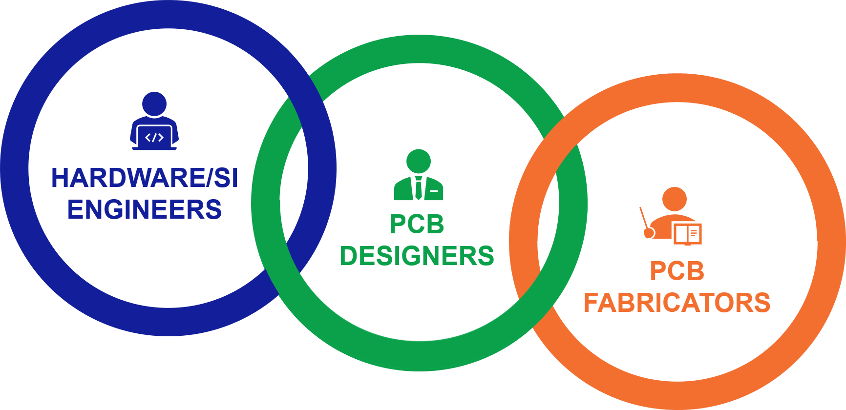
Z-zero offers a comprehensive software solution to solve the gap between hardware design teams and their PCB fabricators. Designed to look and feel like a spreadsheet, Z-zero's software enables hardware design teams to design, validate and automate their PCB design with detailed features for impedance and loss simulation.

2012
Z-planner Enterprise, Z-planner Designer and Z-solver software products have been in development since 2012. The company was officially established in 2016.

Redmond, Washington
With software developers and engineers working in various locations around the world, Z-zero is headquartered in Redmond, Washington, USA.

Founder, Bill Hargin
With 25 years of experience in PCB design, laminate selection, and signal integrity analysis, Bill was a pioneer with HyperLynx, the most widely used signal integrity software solution in the world.
 Our Mission is to reduce schedule delays and rework in the PCB development workflow, streamlining stackup design and validation processes, getting better products to market faster and saving hundreds of thousands of dollars in the process.
Our Vision is to see stakeholders in high-speed PCB workflows get their products to market faster and with higher reliability across multiple hardware OEMs, PCB fabricators, and laminate manufacturers.
 “Survival in the world of high-speed design requires accurate prediction of electrical performance based on design and material properties. Z-zero’s focus on accurately modeling the detailed elements of PCB stackups is a valuable contribution to the industry.”
—Dr. Eric Bogatin, industry pioneer, founder of BeTheSignal, and author of the popular text, “Signal and Power Integrity – Simplified,” “Principles of Power Integrity for PDN Design - Simplified: Robust and Cost Effective Design for High Speed Digital Products,” and “Bogatin’s Practical Guide to Transmission Line Design and Characterization for Signal Integrity Applications.”
 “In our PCB design flow, we have very strict electrical and mechanical requirements that we need to manage across 20+ layers for most designs. Until now, we haven’t found a software solution that was able to capture the layer of detail that we require in our design process. We’ve found that Z-zero software reduces the time it takes us to specify and validate fabricator stackups. We can evaluate three different stackups in an hour, rather than a day, and it significantly reduces the amount of back-and-forth communication required with our fabricators and NPI team.”
—Dr. Jayaprakash Balachandran, Senior Technical Leader, Signal Integrity Engineering, Cisco
Current Market Issue
Years ago, Bill recognized a serious gap in PCB design flows − requiring significant manual intervention. Manual intervention takes time and introduces an opportunity for errors, which often compromises product performance, as well as introducing costly project delays and rework.
Bill saw engineers and fabricators manually entering stackup descriptions into spreadsheets; and he saw signal integrity (SI) analysts re-entering the stackup information into SI simulators. This is the gap.
Engineers often build their own stackup spreadsheets using Dk and Df values from datasheets, while ignoring resin content and frequency. Then they rely heavily on third-party PCB fabricators to resolve final-implementation details with stackup and materials long after simulations were performed − often with data that differs from the as-fabricated printed-circuit board.
Information is sometimes lost between the spreadsheets and the simulators. Critical material details, important to laminate manufacturers and PCB fabricators, are often overlooked by hardware engineers and SI analysts because the information is in multiple formats using different software tools.
Solution
Z-zero bridges this gap and automates information transfer between the functions (CAD design, hardware engineers, SI specialists and PCB fabricators in the PCB design, validation and new product introduction (NPI) workflow.
Where our Name Comes From
Just like a classic album cover or a PCB stackup, there are layers to the Z-zero name and logo that may not be apparent at first glance. Z-zero, usually represented as Z0 or Zo, represents the resistance to the flow of electromagnetic energy along a transmission line or through a component. Aligning impedances along a transmission-line path–through PCB traces, connectors, and cables–is fundamental to signal integrity. That’s the Zo part.
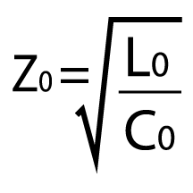 The Z in Z-zero also represents the fact that everything we do is in the Z-direction within a PCB. Electric fields (E-fields) in a PCB–between transmission lines and power and ground planes–are oriented normal to conductor surfaces, with the heaviest concentration of E-fields, composed of inductances and capacitances in the Z-direction, resulting in what we know as impedance.
If you like multiple meanings for otherwise simple things, the word “Zero” has “Zo” on either end, with Er (relative permitivitty; aka: dielectric constant) in the middle. Did we think of all of this when selecting a company name and designing the logo? Actually, yes − If you like depth and careful consideration of details, you’ll probably like our software too!
Contact Us To Learn More
Z-zero, based in
Redmond, Washington, develops
PCB stackup planning and
material-selection software
for electronic-system design.
![]()
![]()