Z-ZERO
SOFTWARE BUNDLES
Two different Z-zero products are available—with either node-locked, USB, floating, or enterprise WAN network licensing.

Z-solver
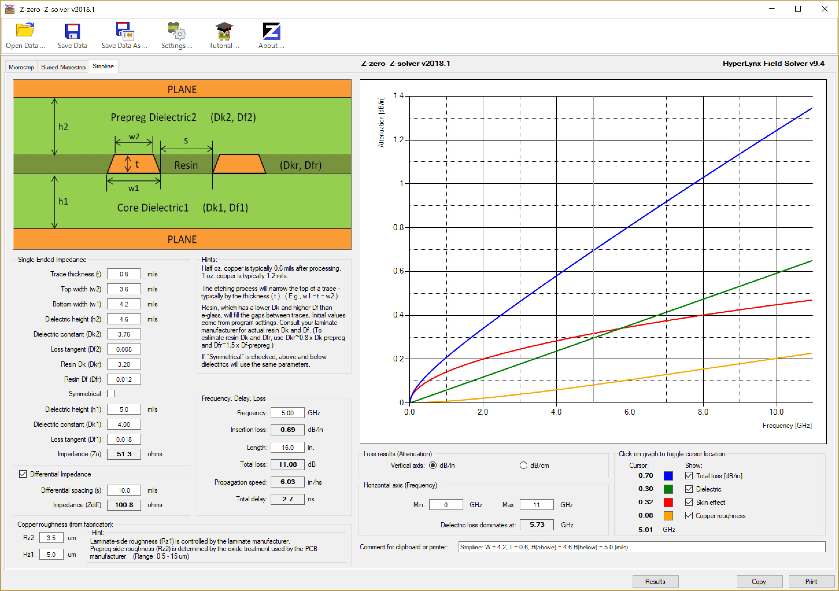
Sometimes you just need quick answers from datasheet parameters and what-if topologies. Z-solver gives designers quick field solver results on impedance, differential impedance, insertion loss, and impacts from copper roughness for microstrip signals, buried microstrip signals and striplines using the time-tested HyperLynx field solver.
- The most reasonably priced path to making tradeoffs between Dk, Df, trace topologies, and spacing.
- Results include impedance, differential impedance, propagation delay, and loss vs. frequency.
- PCB impedance and loss-planning tutorial.
Z-planner
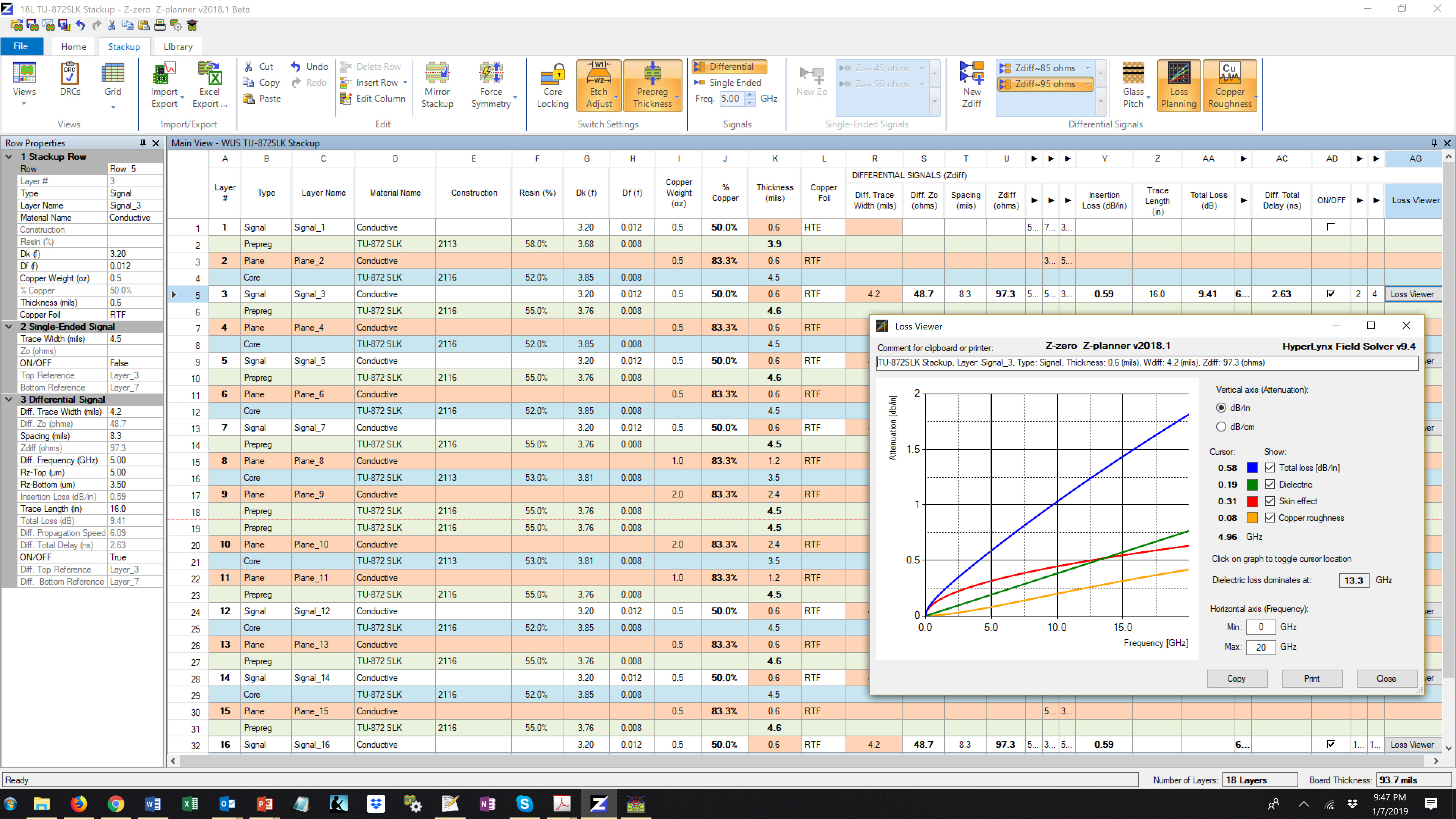
Z-planner is a field-solver based PCB stackup planning and materials selection tool that’s optimized for hardware engineering teams—including just about everything you can think of for designing stackups, including a lossy field solver, an extensive dielectric library, and interfaces to popular signal integrity tools.
- Solve for Zo, Zdiff, insertion loss, and propagation delay.
- Generic stackup library and Stackup Wizard get you started quickly.
- Industry leading accuracy and ease of use.
- Stackup design and PCB material-selection tutorial.
- Includes Z-solver.
PCB Materials
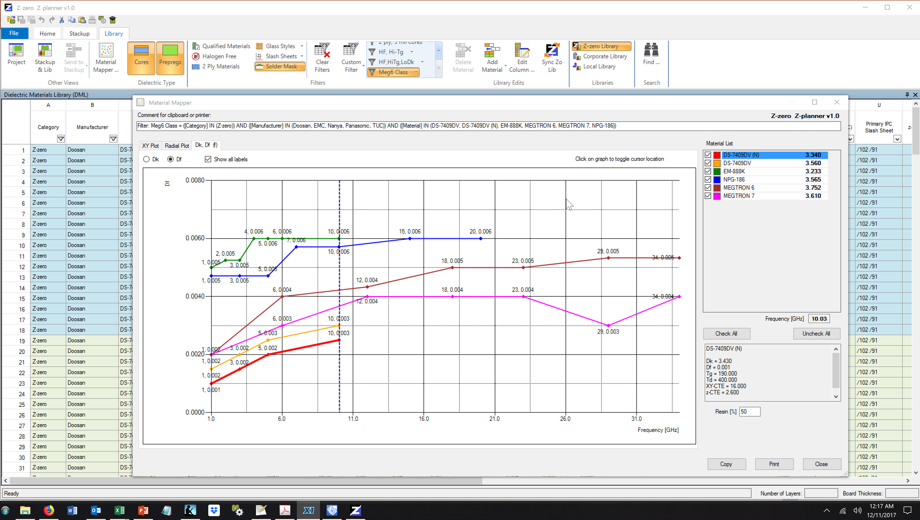
The Dielectric Materials Library provides a central administrative environment for managing and deploying qualified PCB laminate materials, including frequency-dependent Dk and Df for major high-speed PCB laminates right out of the box.

- Use generic or manufacturer-specific material parameters.
- Central administrative environment for managing and deploying qualified PCB laminate materials.
- Frequency-dependent Dk and Df for major high-speed PCB laminates out of the box.
- Filter and sort on every material parameter you can think of.
- Material Mapper ™ allows you to visualize and compare material parameters—in support of your material-selection process.
Industry-Leading Analysis:
The foundation for signal quality—and signal-integrity analysis—is the PCB stackup; and yet detailed design of the PCB stackup is often handled by the PCB fabricator late in the design and prototyping process, long after signal-integrity simulation and analysis should have taken place. Here are some of the patent-pending analysis features in Z-zero software:
- Loss planning, including copper roughness — Layer by layer calculation of loss as a function of geometry, Df, copper roughness on both sides and frequency.
- Automated tracking of glass-reinforcement pitch — for mitigating glass-weave skew (aka: fiber-weave effect).
- Etch effects (aka: trapezoidal traces) — The ratio of the prepreg vs. the core side of a signal layer can be controlled across all stackups by default, or individual stackups.
- Reference signals to non-adjacent planes for field-solver impedance calculations.
- Detailed modeling of solder masks — Enabling increased accuracy in microstrip impedance calculations.
- Show/edit Vias — Document via diameters and layer connectivity for fabrication, including aspect ratios.
- Stackup DRC’s — Automatically detects errors, including symmetry violations, incorrect stackup sequencing, etc. in PCB stackups.
- Propagation delay simulation — Automatic calculation of signal propagation delay. Results are available in both delay/inch, and total delay for a signal path.
- Pressed prepreg thickness — Automatic adjustment of board and prepreg thickness due to prepreg flow in fabrication.
- Multiple differential pairs — Unlimited named differential impedance calculations on any signal layer.
- PCB stackup import/export utilities — for popular signal integrity software, enabling design reuse and more accurate simulation results.
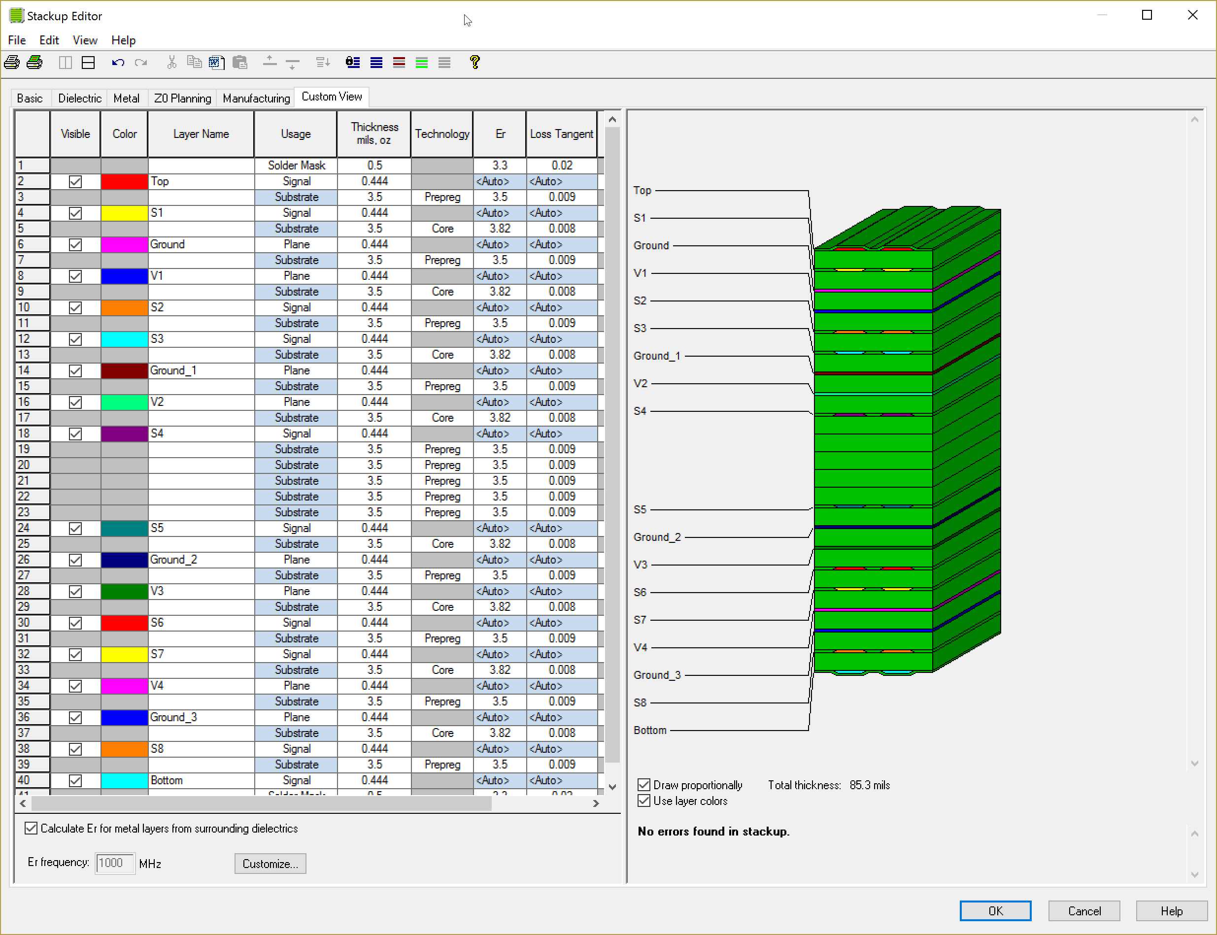
Industry-Leading Ease of Use
Customizable project views, allowing each user to customize the fields, parameters, and preferences for working with PCB stackup design.
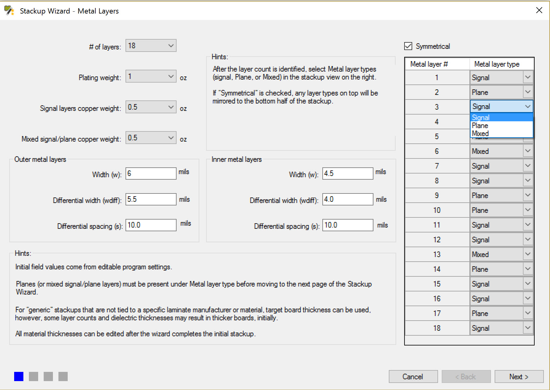
- Stackup Wizard allows you to create a stackup of any thickness and layer count, enabling automated creation of generic stackups, or stackups based upon product or material-parameter searches of the dielectric materials library.
- Excel export allows easy stackup documentation in a familiar, portable output format.
- Unlimited named differential impedance calculations on any signal layer.
- Customizable project views, allowing each user to customize the fields, parameters, and preferences for working with PCB stackup design.
- Horizontal line of symmetry in the stackup can be turned on or off.
- Core locking can be turned on or off—enabling you to copy/paste or drag and drop a core dielectric from the library together with associated copper layers.
