Z-PLANNER DESIGNER™
Z-planner Designer™
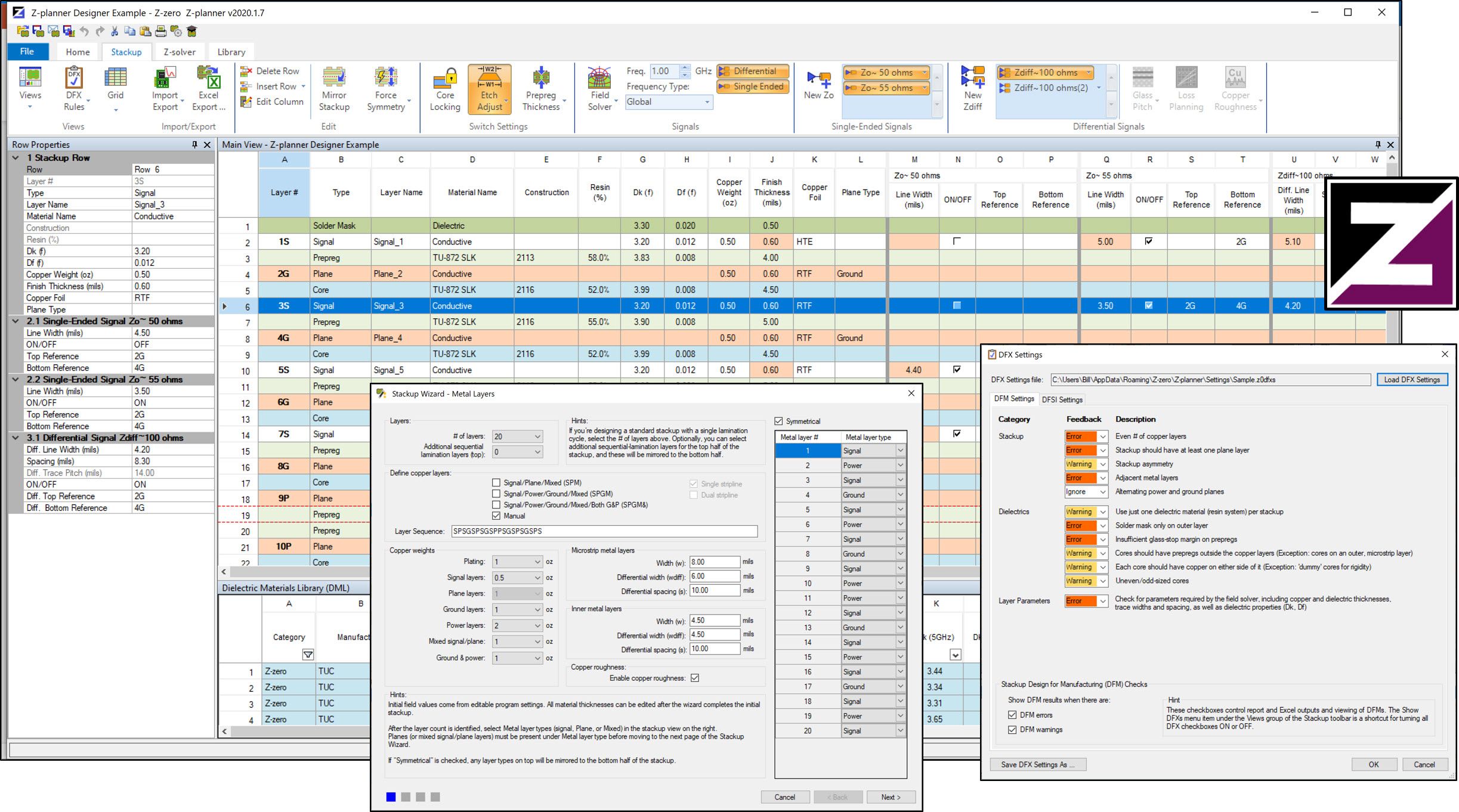
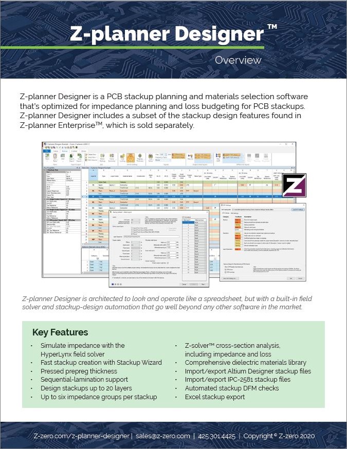
Z-planner Designer is PCB stackup planning and materials selection software that’s optimized for impedance planning and loss budgeting for PCB stackups. Z-planner Designer includes a subset of the stackup design features found in Z-planner Enterprise™, which is sold separately.
Z-planner Designer Includes:
- Everything necessary for designing stackups up to 20 layers and selecting materials
- Automated calculation of width/spacing
- HyperLynx field solver—simulating impedance and dielectric loss
- Z-solver™—detailed cross-section analysis, including impedance, loss, and S-parameter export
- DFM rules management and checking
- A stackup-design focused subset of the features found in Z-planner Enterprise

Benefits of Z-planner Designer
- Simulate impedance with
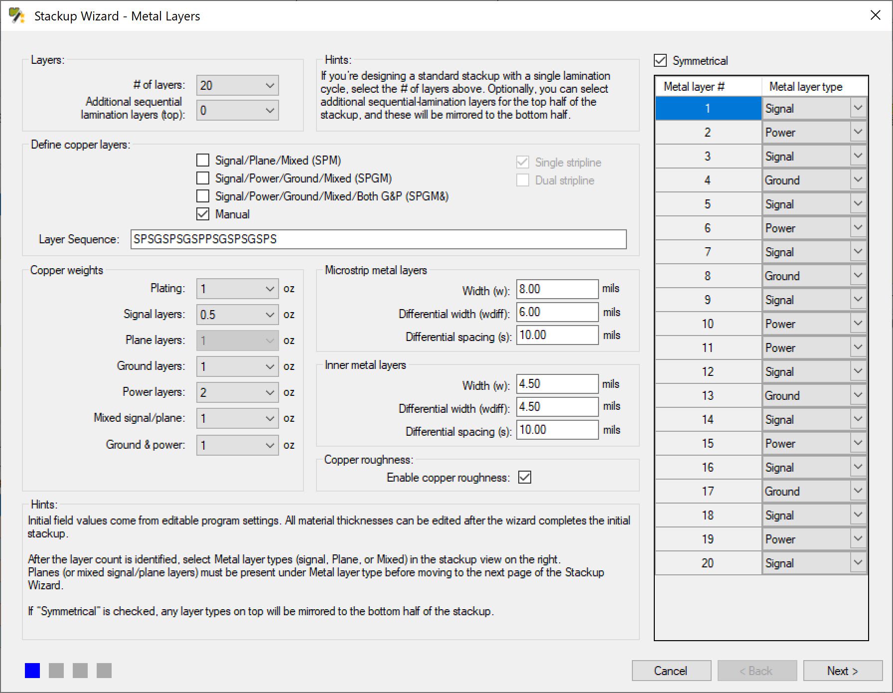
the HyperLynx field solver - Fast stackup creation with Stackup Wizard
- Pressed prepreg thickness
- Sequential-lamination support
- Design stackups up to 20 layers
- Up to six impedance groups per stackup
- Z-solver™ cross-section analysis, including impedance and loss
- Comprehensive dielectric materials library
- Import/export Altium Designer stackup files
- Import/export IPC-2581 stackup files
- Automated stackup DFM checks
- Excel stackup export

Dielectric Material Library
- The industry’s largest dielectric-materials library, including laminates from AGC-Nelco, EMC, Doosan, ITEQ, Nanya, Panasonic, Shengyi, TUC, and Ventec
- Full accounting for frequency, resin content, glass style, and pressed prepreg thickness
- Z-zero library, spreadsheet-manageable Corporate library, and local (desktop) libraries
- Library updates as they become available over the Internet
- Built-in filters for common constraints like halogen-free materials, dual-ply cores, and a complete set of the IPC 4101 slash sheets
- Custom filters using any mechanical or electrical material parameters
- Material Mapper™ includes comprehensive plots, including Dk, Df, Tg, Td, z-CTE, and x-y CTE
- Built-in interface to Z-field™ for direct Dk and Df measurements from laminates from 1-20 GHz
- Z-planner Enterprise (sold separately) also includes Material Matching™ for automated stackup redesign based on material parameters


