Z-ZERO PRODUCT OVERVIEW
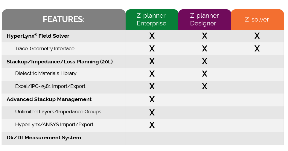
Z-zero has three products, listed below and shown in the high-level feature checklist. Z-zero products enhance the stackup design process by providing an accurate field solver, a loss-planning environment, and a complete dielectric materials library — seamlessly interfaced to the most popular signal-integrity software.
Although conceptually similar tools exist, Z-zero is the only software provider that eliminates the major workflow communication issues between hardware design teams and the PCB supply chain. Communication of specifications and material properties becomes automated using Z-zero tools, eliminating manual re-entry of data.
Z-zero Product Checklist

Z-planner Enterprise™ is a field-solver based PCB stackup planning and materials selection software that’s optimized for both the design of the PCB stackups and the management of the stackup design as part of the PCB design flow. Z-planner Enterprise also includes Z-solver and Z-planner Designer. Click here to learn more.
Z-planner Designer™ is PCB stackup planning and materials selection software that’s optimized for impedance planning and loss budgeting for PCB stackups. Z-planner Designer also includes Z-solver and a subset of the stackup design features found in Z-planner Enterprise™, which is sold separately. Click here to learn more.
Z-solver™ provides the most reasonably priced path to making tradeoffs between Dk, Df, trace topologies, and spacing. Results include impedance, differential impedance, propagation delay, and loss vs. frequency, for quick, accurate answers from datasheet parameters and what-if topologies. Click here to learn more.
