Z-SOLVER™
Z-solver
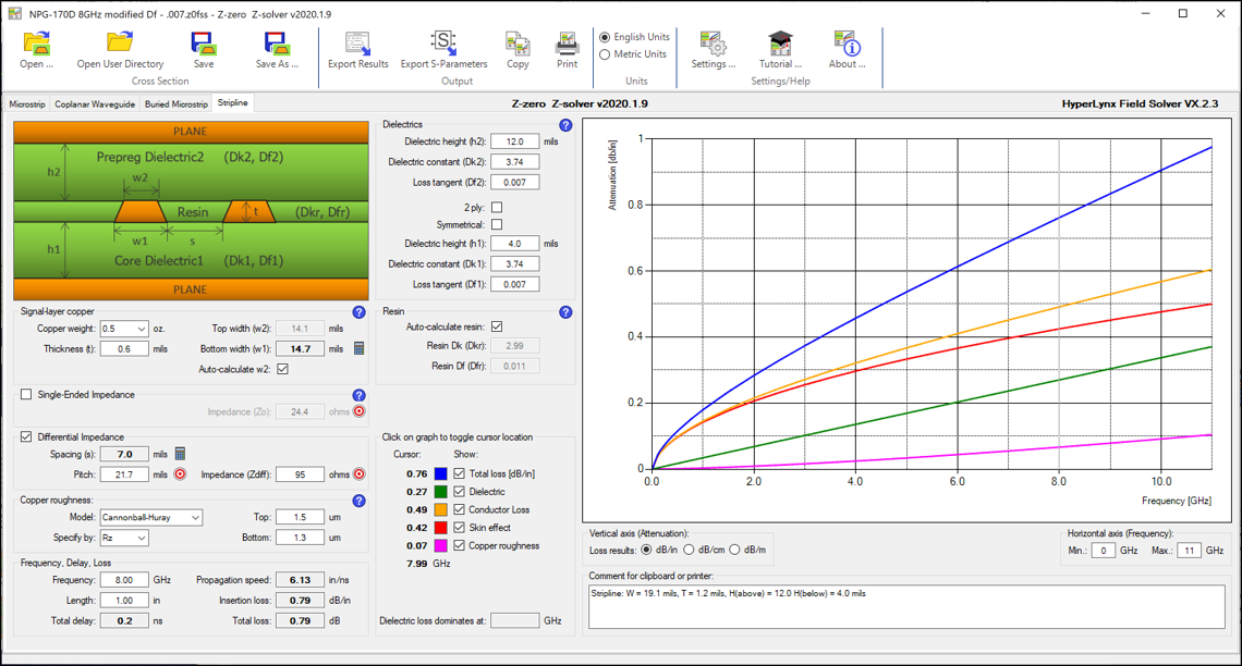
Sometimes you just need quick answers from datasheet parameters and what-if topologies. Z-solver™ provides the most reasonably priced path to making tradeoffs between Dk, Df, trace topologies, and spacing. Results include impedance, differential impedance, propagation delay, and loss vs. frequency.


Z-solver Includes:
- Everything necessary for simulating detailed PCB stackup cross sections, including microstrips, buried microstrips, coplanar waveguides, and striplines
- HyperLynx field solver—simulating impedance, as well as dielectric and copper losses
- Cross-section reuse, including the ability to save, open, or e-mail stackup cross sections
- Automated impedance goal seeking
- Highlighting of inter-connected parameters
- Export capabilities—including S-parameters with channel characteristics for design reuse, text output, including channel parameters such as capacitance, inductance, and impedance matrices
- The ability to easily toggle between English and metric units
- Graphical and numeric analysis of channel loss
How Z-solver is used:
There are a lot of factors to juggle to stay on top of the parameters that contribute to loss, including frequency, copper weight, resin system, glass characteristics, dielectric thickness, trace width, copper roughness, and fabricator processing all contribute to the discussion.

Co-planar waveguide
It’s common in high-speed PCB design to build test boards with defined geometries across multiple laminate vendors, materials, and fabricators, but the process of doing so takes about six months from concept to completion. In today’s design environment, who can wait that long for concrete answers? A lot of hardware design teams don’t have the luxury of long lead times, where straightforward questions take multiple months to answer.

Stripline view
Z-solver allows designers to make tradeoffs early in the system-design process, including frequency, interconnect loss budgets, and the knobs that designers control, including resin system, cost, copper roughness, and trace length.
Key Benefits of Z-solver:
- HyperLynx field solver
- Detailed cross-section analysis of
microstrips, buried microstrips, co-planar
waveguides, and striplines - Single-ended and differential impedance
- Automated impedance goal seeking
- Propagation speed and total-delay simulation
- Simulate insertion loss, total channel loss, and a detailed breakdown of dielectric and conductor loss, skin effect and copper roughness, including Cannonball-Huray
- S-parameter channel-model export
- Solder mask and dual-ply prepreg modeling
- Detailed modeling of etch effects

Download the Datasheet:
Learn More About Z-zero's Other Products
Z-zero, based in
Redmond, Washington, develops
PCB stackup planning and
material-selection software
for electronic-system design.
![]()
![]()