
DATE: January 30 - February 1, 2024
LOCATION: Santa Clara Convention Center, Santa Clara, CA

DATE: October 8-11, 2024
LOCATION: Santa Clara Convention Center, CA
DesignCon is the premier high-speed communications and system design conference and exposition, offering industry-critical engineering education in the heart of electronics innovation — Silicon Valley.
Bill Hargin is giving a stackup design workshop at DesignCon 2024. Click here for details.
You can use his promo code REFER23 for 15% off a conference pass or free admission to the expo hall.
Register here.
For more than 30 years PCB West has trained designers, engineers, fabricators and, lately, assemblers on making printed circuit boards for every product or use imaginable. More than 2,000 designers, fabricators, assemblers and engineers register and more than 100 companies exhibit each year at the four-day technical conference and one-day sold-out exhibition. From high-reliability military/aerospace to cutting-edge IoT and wearables, there’s something for everyone involved in the electronics supply chain. This is one show you cannot afford to miss.
Previous Events

Engineering the Power Distribution Network

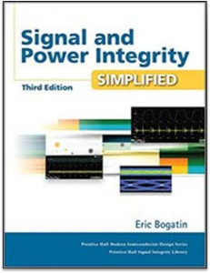
Dr. Eric Bogatin, author of the best-selling book, "Signal and Power Integrity Simplified" is currently a Signal Integrity Evangelist with Teledyne LeCroy and the Dean of the Teledyne LeCroy Signal Integrity Academy at Be The Signal. Additionally, he is an Adjunct Professor at the University of Colorado-Boulder in the ECEE Dept., and technical editor of the Signal Integrity Journal.
Abstract:
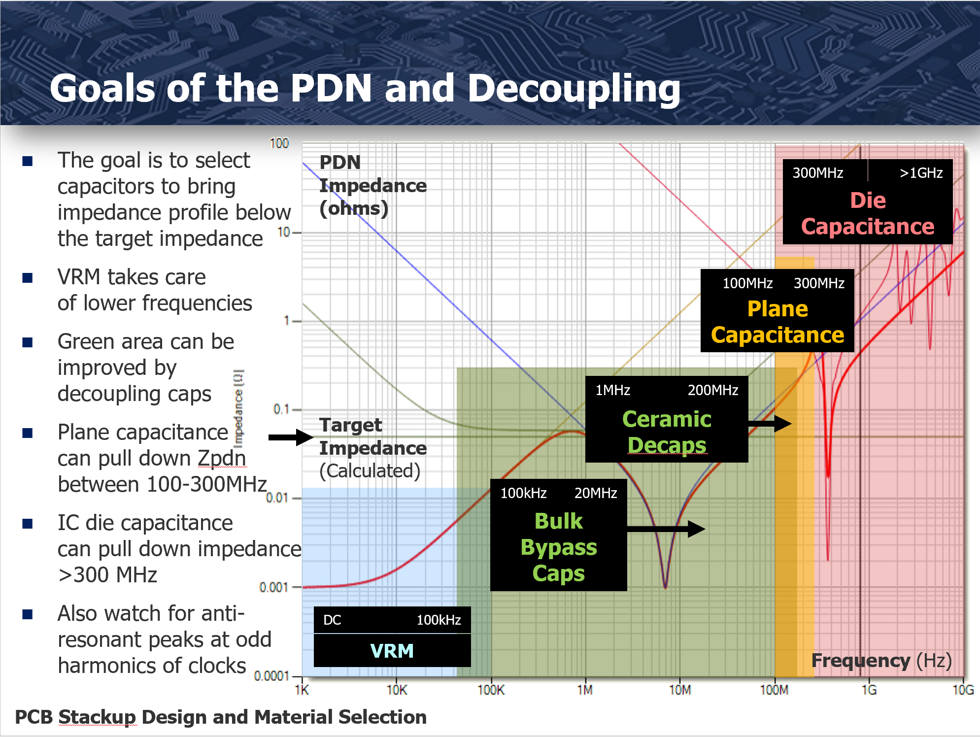
The power distribution network (PDN; sometimes also called the power delivery network) consists of all the interconnects from the voltage-regulator module (VRM) to the pads on the chip and the metallization on the die that locally distributes power and return current. This includes the VRM itself, the bulk decoupling capacitors, the vias, the traces, the planes on the circuit board, the additional capacitors added to the board, the solder balls or leads of the packages, the interconnects in the packages mounted to the board, the wire bonds or C4 solder balls, and the interconnects on the chips themselves.
The first and primary role of the PDN is to keep a constant supply voltage on the pads of the chips and to keep it within a narrow tolerance band, typically on the order of 5%. This voltage has to be stable, within the voltage limits, from DC up to the bandwidth of the switching current, typically above 1 GHz.
In this webinar, Eric explores the entire PDN ecosystem, including both board and system-level tradeoffs.
Moderated by Bill Hargin, Director of Everything at Z-zero.
Embedded Capacitance for PDN Design
In this webinar moderated by Bill Hargin, Director of Everything at Z-zero, Istvan Novak of Samtec and John Andresakis of DuPont presented power distribution network (PDN) design and where embedded-capacitance fits into the picture.
What you'll learn:
- Why we care about PDN design. (Who cares and why.)
- How embedded, interplane (low-inductance) capacitance fits into the overall PDN design scheme.
- When to incorporate embedded capacitance into a stackup and where high-Dk laminates fit into the picture.
- A brief introduction of DuPont's Interra HK04 product line.
Presenters:
 Istvan Novak is a Principle Signal and Power Integrity Engineer at Samtec, working on advanced signal and power integrity designs. Prior to 2018 he was a Distinguished Engineer at SUN Microsystems, later Oracle. He worked on new technology development, advanced power distribution and signal integrity design and validation methodologies for SUN's successful workgroup server families. Istvan holds 25 patents, is the author of two books on power integrity, teaches signal and power integrity courses, and maintains a popular SI/PI website.
 John Andresakis is Technical Marketing and Business Development Leader in DuPont’s Electronics and Imaging Business. He is a 20+ year veteran of the PCB industry, having worked from front-to-back across the PCB supply chain. At DuPont, John works with OEMs to determine their needs and helps direct R&D efforts to meet those needs.
Moderated by Bill Hargin, Director of Everything at Z-zero.
Glass-Weave Skew - Part 2 - Mitigation Methods
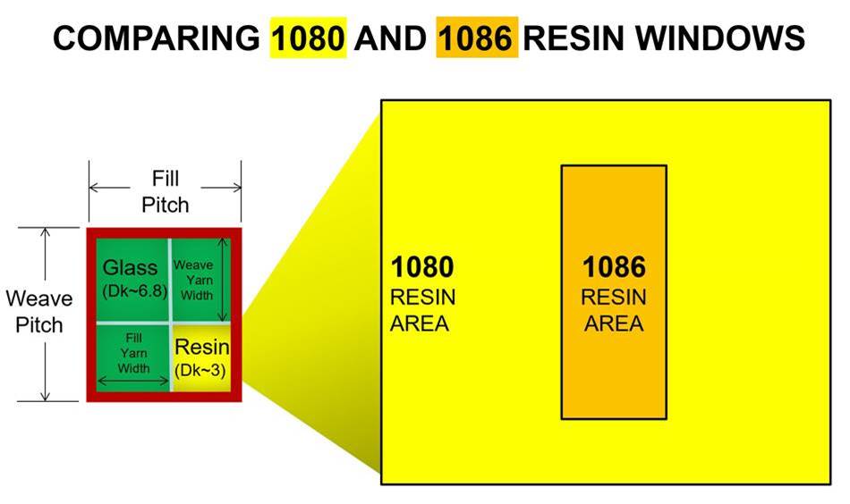
A serial link’s differential-skew budget shrinks as bit rates increase. For example, a 1 Gbps (500 MHz) signal would have roughly 250 ps of skew tolerance. That’s a wide window, and why most engineers didn’t need to worry about GWS 20+ years ago. Fast forward to 10 Gbps (5 GHz), and the skew tolerance will decrease proportionally to around 25 ps—or even narrower with fast transmitter edge rates.
In Glass-Weave Skew Part 1, we covered the causes of GWS, while doing a deep dive into the question, "Who cares?" (E.g., Asking whether it's safe to ignore it.)
In Glass-Weave Skew Part 2, we went into more detail on possible solutions, with an eye toward cost and future-proofing your designs, preventing design and manufacturing teams from getting blind-sided by this issue.
Glass-Weave Skew - Part 1 - Who Cares?
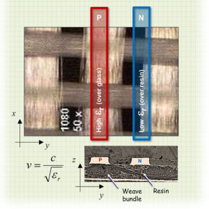
Everything that happens in the process of building a PCB works against signal quality. Glass-Weave Skew (GWS) – also referred to as the Fiber-Weave Effect (FWE) – is one such issue that seems to be misunderstood on a pretty wide scale. Glass-weave skew is an increasingly important problem above 10 Gbps.
In this presentation, we will cover the causes of GWS, while doing a deep dive into the question, “Who cares?” (E.g., Asking whether it's safe to ignore it.)
In Glass-Weave Skew Part II, the follow-on session on April 29, we’ll go into more detail on possible solutions, with an eye toward cost and future-proofing your designs, preventing design and manufacturing teams from getting blindsided by this issue.
Apples-to-Apples PCB Laminate Characterization
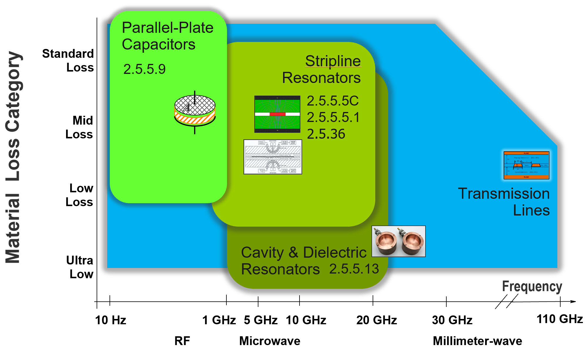
Employing accurate material parameters in PCB design is critical to electrical performance, ensuring both signal and power integrity. PCB laminate manufacturers publish construction tables with resin-content and permittivity (Dk, Df) specifications. How can design teams ensure that they have an “apples-to-apples” comparison across multiple laminate systems, constructions, and data sources?
In this presentation, we’ll demonstrate a quick and direct method of acquiring actual dielectric constant (Dk) and loss tangent (Df) values from the same materials that will be used by your fabricator. This replaces guesswork and trust with actual values acquired from your own bench.
