Apples-to-Apples Material Characterization for High-Speed PCB Design

Engineers invest tens to hundreds of thousands of dollars in signal integrity simulation software—the goal being to gain an accurate understanding of how signals are going to behave in the final product. But how do you do that early in the design process without reliable, verifiable electrical properties for the dielectrics incorporated into your design?
Simulating tens to hundreds or even thousands of signals on a circuit board without first ensuring that the input information is accurate is a garbage in, garbage out exercise. Employing accurate material parameters in PCB design is critical to electrical performance, including both signal and power integrity.
On the front end of a design project, signal integrity analysis is typically based on the available laminate data from copper-clad laminate (CCL) or printed circuit board (PCB) manufacturers. For this purpose, laminate manufacturers provide high-level datasheet information and publish construction tables with resin-content, dielectric constant (Dk), and loss tangent (Df), also known as dissipation factor, specifications. To what degree can this data be trusted and what are the implications for signal integrity?
And when making material decisions, how can design teams ensure that they have an “apples-to-apples” comparison of electrical properties across multiple laminate systems, constructions, and data sources—particularly when laminate manufacturers use different test methods to characterize their laminates? Each permittivity test method has known quirks and biases that are large enough to raise concern when choosing materials or designing circuit boards.
While design teams may measure impedance and insertion loss on test vehicles at appropriate frequencies for their target applications, PCB fabricators typically plan stackups at 1 GHz. To what degree does this practice impact actual designs, operating at their target frequencies?
Designing for Impedance and Insertion Loss
When selecting laminates and planning stackups for target impedances and loss, hardware teams delegate much of the process to their PCB fabricators, who in turn make assumptions regarding frequency and retained copper (%) on signal layers. This may work fine at 1 GHz, in fact, but at higher speeds hardware engineers require material parameter accuracy to within 5 percent for pre-prototype signal integrity simulations. In this article, our focus is on more-accurately characterizing Dk and Df.
Background of Dk and Df Measurement Methods
Most characterization methods used by CCL manufacturers come from industry or standard associations like the IPC and ASTM. Such methods have been shown to be gauge capable, ensuring reproducibility, but in most cases, the total measurement uncertainty is unknown and not traceable to a national metrology institution like NIST. Further, CCL production control relies on a particular dielectric test method most suited to the manufacturing environment, but a production test method may not provide a Dk/Df measurement suited for the design environment. As a result, there is no way to know whether a vendor-provided Dk/Df measurement is an accurate representation of the material properties to use in signal integrity simulation.
To compound the confusion, there is no industry consensus on which production test method to use. CCL manufacturers and customers are allowed to agree upon the test method used for quality control and material acceptance. Consequently, the IPC TM-650, includes 12 different permittivity test methods. Datasheet Dk/Df values will not correlate apples-to-apples across laminate manufacturers that use different test methods.
Another distinction between CCL and fabricated PCB test methods ties to copper conductors. In CCL testing, the copper, or the effects of the copper, are totally removed from a single sheet of laminate material to report only the permittivity of just the dielectric. In fabricated PCB testing, transmission line devices are used to test performance of fabrication including copper effects.
We recommend dielectric test methodologies for apples-to-apples material comparisons and initial design efforts prior to prototyping—followed by transmission line based ;approaches using as-built constructions later in the design process, leading up to formal part-number qualification.
E-Field Orientation
Electric fields in a PCB between transmission lines and power and ground planes are oriented normal to laminate surfaces. The heaviest concentration of E-field lines are in the z-direction, or “out of plane,” as opposed to x-y direction,or “in-plane.” Because of this, dielectric measurements for signal and power integrity applications should also be performed out of plane. Unfortunately, dielectric material parameters provided by many CCL manufacturers today are acquired with both in-plane methods and out-of-plane methods.
Dk and Df Measurement Methods Used in Laminate Tables
To make matters even more confusing, laminate manufacturers may use:
• One test method for datasheets and another for their Dk/Df tables.
• One test method at 1 GHz and another test method above 1 GHz.
• One test method for Dk and another test method for Df.
We discovered all of the above variants in the laminate manufacturers we studied as well as a subset of the 12 different IPC test methodologies—the most common of which are summarized in Figure 1.
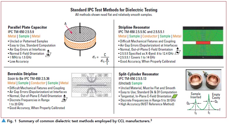
Enhanced Stripline Test Method
The stripline-based test methods have the advantage of producing the out-of-plane Dk and Df results that signal-integrity engineers are looking for, but with some inherent disadvantages, including the frequency limitations of IPC TM-650 2.5.5.51 and 2.5.5.5.12 and due to the fact that individual test sites are left to themselves to cobble together equipment details from multiple sources, including connectors, cabling, fixtures, and calibration. As a result, no two test systems are identical. With a goal of providing a remedy for this, the authors are collaborating on integrating a commercial stripline resonator test system with a commercial stackup design tool.
In the commercial stripline resonator shown in Figure 2, the IPC stripline methods are modified to more fully and consistently correct for copper losses and connection responses to report a corrected Dk and Df of only the dielectric region of the test specimen, uninfluenced by the resistive losses of the conductors. The fixture measures fullyetched pieces of dielectric with separate copper foils, as in the Type A specimens of IPC TM-650 2.5.5.5.1.2
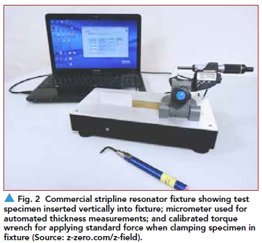
Calibration involves the ex-situ characterization of the fixture’s copper foils in an air-gap transmission line resonator and does not rely on published resistivity or copper roughness models. The system provides Dk and Df of just the dielectric region with Dk uncertainties within 5 percent and Df uncertainties within 0.001. Additionally, this method provides a high degree of repeatability (better than 2 percent for Dk and better than 0.0005 for Df) for testing differences between dielectrics in the same lab.
Measurement Results
As part of our journey toward the “ideal” dielectricmeasurement system, our goal was to gain insight to how closely published CCL manufacturers’ table values for Dk(f) and Df(f) correlate to our calibrated measurements of the dielectric’s Dk and Df from 1 to 20 GHz.
Within specific CCL manufacturers, published Dk’s varied by ±10 percent from our reference measurements3—a 20 percent variation from minimum to maximum. For signal integrity purposes, it would be advantageous to remove this additional source of uncertainty—both during new product introduction (NPI)/prototyping activities and in volume production.
Dk and Impedance
To provide an idea of the impedance implications associated with accurate Dk values, Figure 3 shows a symmetrical differential stripline model with 5-mil thick dielectrics and 5-mil wide traces.
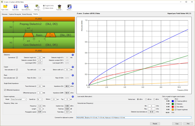
Fig. 3 Measured laminate properties produce a single-ended impedance of 48Ω, a differential impedance of 92.8Ω and iinsertion loss of 0.95 dB/in at 10 GHz. Simulated in Z-zero Z-solver software with the HyperLynx® field solver.
Published: Incorporating a published Dk of 3.74 produced a 50.8Ω simulated single-ended (SE) impedance and a 97.2Ω differential impedance on 12-mil spacing.
Measured: Using the measured Dk value at 10 GHz for a laminate in our study, the simulated SE stripline impedance result was 48.5Ω, with a 92.8Ω differential impedance.
A design may be able to survive a 4.5Ω difference, but this difference will be in addition to other tolerances and manufacturing variations that must be accounted for, which can pose problems if all of the variance works in the same impedance direction. And impedance mismatches— assuming targeting target of 100Ω differentially—cause risetime degradation that contributes to eye closure. Our view is that giving away this accuracy when it is so easily avoidable is not a good design practice.
Df and Insertion Loss
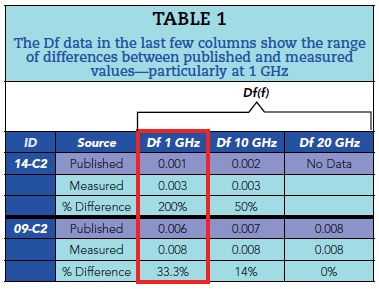
One of the more significant findings in our research is the degree to which published Df values tend to diverge from our calibrated stripline-resonator results. These differences vary in magnitude, but always in the same direction: our calibrated stripline-resonator measurements were always higher than vendor-published values. The Df differences were particularly striking at 1 GHz—ranging from 33 percent for material 09-C2 to 200 percent for material 14-C2, as shown in Table 1.
To get an idea of the propagation-loss implications for underestimating Df, we will use the same stripline configuration noted in Figure 3, assuming copper foil with Rz = 2 μm roughness on the laminate and processing on the prepreg side that results in Rz = 1.5 μm.
Published: Incorporating a published Df of 0.006 produced an insertion loss of 0.72 dB/in at 10 GHz.
Measured: Using the measured Df value of 0.010 at 10 GHz for a laminate in our study, resulted in an insertion loss of 0.95 dB/in at 10 GHz, as shown in Figure 3.
Multiply these values by a 10 in. interconnect length and we are talking about almost a 2.5 dB difference. That is not a long signal path and the unplanned loss delta is enough to cause headaches, especially for longer run lengths. There is a cost element, as well. In this example, you paid for 0.006 and received 0.010. That is a caveat emptor (“let the buyer beware”) moment. The only foolproof way for engineers to know that they are getting the loss performance that they are paying for is to measure dissipation factors at frequencies of interest on their own test benches and in the production environment.
Dielectric method inter-comparison studies4 have shown that the methods identified in the CCL manufacturers’ datasheets are capable of Df measurements to within 0.001, so it is not immediately clear where the under-reporting of published Df values is coming from. One possibility is that the variation may be rooted in the fact that a given lab may not have access to well-established verification standards that would tell a measurement technician whether their equipment and methodology are dialed in properly. The fact that some of the published numbers are so far off seems to imply a broader set of causes than simply calibration, however.
Since dielectric loss is represented with the dissipation factor, there is a significant risk that the loss-budgeting process can be compromised through the use of potentially under-reported dissipation factors. The potential problem is further exacerbated by the fact that transmission line loss also varies to first order with the square root of the dielectric constant. Knowing these values—at the proper frequencies of interest—is critical when optimizing material choices where dielectric loss and material cost are concerned.
Conclusions
Published Dk values varied ±10 percent from our reference measurement results—a 20 percent range from minimum to maximum. Dk variation and uncertainty needs to be further measured and modeled for improved signal integrity analysis. It is not immediately clear why published values for Dk differ significantly from the calibrated, out-of-plane results from the authors’ own lab measurements. Manufacturing variation, slight formulation changes, sample size—both for published values and as a matter of ongoing sampling, and measurement equipment calibration are all considerations.
Our research raises serious questions regarding CCL manufacturers’ published Df values. Across all vendors and measurement methods, published Df values fell significantly below our reference measurements. Differences at 1 GHz proved to be particularly significant. Since material selection (cost vs. loss) and loss planning are both based upon Df values, this has potentially critical implications, both for signal integrity and cost control in volume production.
Using the stripline resonator technique highlighted in this article, the same Dk and Df test method can be used for comparisons during the laminate selection process, to acquire valid Dk and Df functions for design, and to monitor the supply chain during production—all with out-of-plane, comparative results. For a reasonable upfront and ongoing investment, the proposed solution provides CCL manufacturers, PCB fabricators, ODMs, and OEM design teams with a means of ensuring that the electrical parameters they are designing with are what they will be getting in volume production, and that they are able to compare laminate properties on an apples-to-apples basis.
References
1. “Stripline Test for Permittivity and Loss Tangent (Dielectric Constant and Dissipation Factor) at X-Band,” IPC TM-650 2.5.5.5, Rev. C, March 1998.
2. “Stripline Test for Complex Relative Permittivity of Circuit Board Materials to 14 GHz,” IPC TM-650 2.5.5.5.1, March 1998.
3. D. DeGroot and B. Hargin, “Apples-to-Apples Laminate Characterization,” DesignCon 2019, Santa Clara, Calif., February 2019.
4. G. Oliver, J. Weldon, J. Coonrod, C. Nwachukwu, D. L. Wynants Sr., J. Andresakis, and D. DeGroot, “Round Robin of High-Frequency Test Methods
by IPC-D24C Task Group,” IPC APEX Expo 2016, March 16, 2016.