Cutting Your Losses Upfront in PCB Design
A methodology for selecting the right material and the right price point.
When I started writing this column a couple years ago, I wondered how much I’d have to say. An experienced media guy told me to watch my inbox for topics and questions that may be of general interest. That turned out to be excellent advice. Here’s one such example.
“What is the best laminate for a loss budget of x dB for y inches? I was thinking in terms of Panasonic Megtron 6 or something like it.”
Megtron 6 is an excellent material, but it’s not cheap and it’s not the only horse in the race. My response was to focus on a loss and material-planning methodology rather than making a firm material recommendation.
Why we care. Everything that improves material performance – in particular, reductions in loss – comes at a price. Loss versus cost is a classic optimization problem. Designers want to pay just enough to meet loss requirements, but not more than they need to.
In the past, speeds were slow, layer counts were low, dielectric constants (aka Dk or Er) and loss tangents (aka dissipation factor, or Df) were high, design margins were wide, copper roughness didn’t matter, and glass-weave styles didn’t matter. We called dielectrics “FR-4,” and their properties didn’t matter much.
As speeds increased in the 1990s and after, PCB fabricators acquired software tools for designing stackups and dialing-in target impedances. In the process, they acquired PCB laminate libraries, providing proposed stackups to their OEM customers, typically late in the design process, including material thicknesses, copper thickness, dielectric constant and trace widths often weeks or months after initial signal-integrity simulation and analysis should have taken place.
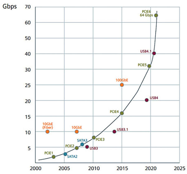
As speeds continued to increase, design margins continued to tighten and OEM engineers began tracking signals in millivolts (mV) and picoseconds (ps). FIGURE 1 shows these trends starting in 2000. Note in particular the PCI Express trajectory. Critical factors for signal integrity now include not only impedance, but loss, copper roughness and glass-weave skew. Indeed, everything that happens in the process of physically building a PCB affects signal quality in a negative way, and the details need to be accounted for across not just one PCB stackup, but across stackups from every PCB fabricator involved with a design.
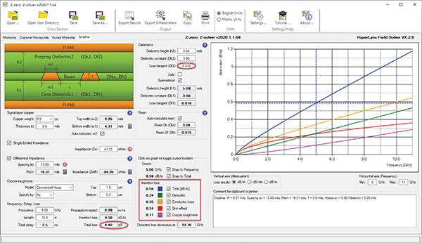
5dB interconnect loss at 5GHz. Let’s say we’re targeting 5dB total interconnect loss at 5GHz for a 15″ stripline run length using 0.5 oz. copper. We’ll ignore vias for this example and just focus on the laminate. Experience says this may require a material that’s indeed in the Meg6 range, but we don’t want to spend more money than we have to, so we’ll start with a loss tangent (dissipation factor, Df) of 0.010 and see where we’re at for a starting point.
FIGURE 2 shows the result, but some explanation is in order. The blue line represents total loss, which is the sum of all other sources of loss. The orange line is conductor (copper) loss, which is the sum of skin-effect loss (red) and copper roughness (magenta). The graph shows loss in dB per inch, resulting in a total interconnect loss of 8.82dB, a good bit above our target of 5.0dB.
The next place I look is the insertion loss box, which is expanded in FIGURE 3. The two biggest contributors to loss here are the skin effect loss and dielectric loss, both at 0.24dB/in. I know we can cut dielectric loss in half by cutting the Df value in half, so let’s give that a try. Changing Df to 0.005 results in a dielectric loss of 0.12dB/in. and a total loss of just over 7.0dB – a significant improvement! Figure 3 also shows loss from copper roughness at 0.11dB/in. is very close to our new dielectric-loss contribution.
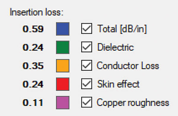
Figure 2 shows the core-side roughness for this hypothetical laminate has an Rz roughness of 5.0µm. This corresponds to what many call RTF, or reverse-treated foil. I happen to know that materials in the 0.005 Df range generally offer smoother copper either by default or as a loss-reduction option. Let’s see what would happen with VLP2 or “very-low profile, 2µm” copper. FIGURE 4 shows this change, along with the resulting total interconnect loss, which is now 5.92dB – much closer to our goal.
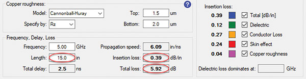
The total insertion loss is now 0.39dB/in. An easy next step toward achieving our 5dB goal is to create a routing rule that reduces the original 15″ to 12″. Let’s make that change and see where we end up.
Voila! Total loss becomes 4.74dB. We now have a Df target for a laminate system, a copper-roughness selection, and a routing rule. That’s a lot of progress early in the PCB design process. We can now begin looking for a material that aligns with these parameters.
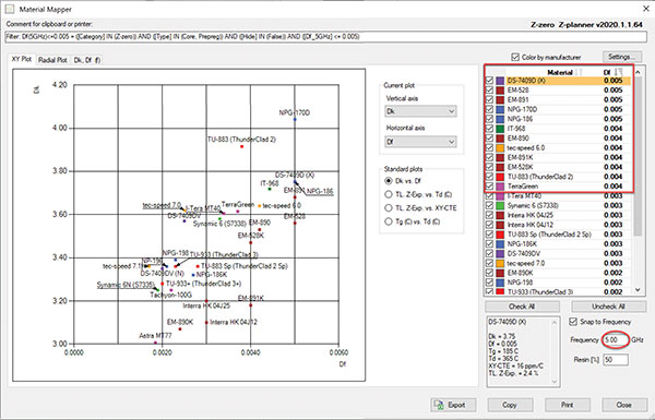
Two good places to initiate that search are with your PCB fabricator(s) or from laminate-vendor data. Several materials that may be worth looking into are shown in FIGURE 5, based on their vendor-published Df numbers at 5GHz.
Wrapping up. If you can make material decisions like this early in the design process, you’ll avoid prototype surprises down the road or paying more than you need to for laminate systems that are overkill for a design. Making these choices early also allows you to avoid initial laminate lead times that can delay prototypes or early production. Because of prepreg shelf-lives, fabricators carry only the laminates they know they can use within six months or less, following a just-in-time approach. As in many other aspects of life, planning means more options and fewer surprises. You can feed that expensive signal-integrity solution Dk and Df data from the actual laminate system you’re planning to use. Moreover, it may allow you to hold to NPI (new product introduction) schedules more consistently, while at the same time relieving some of the pressure you put on PCB suppliers to make up for poor planning. Everyone wins!
PCB East: The original East Coast technical conference and exhibition! Returning to the Boston suburbs in May 2021!
Great site you have here.. It’s difficult to find quality writing like yours nowadays. I seriously appreciate people like you! Take care!!
Thank you