Dk and Df Characterization Methods for PCB Laminates – Part III
Part three of our series on Dk and Df characterization looks at stripline methods.
This is part three in a series that examines how the industry at-large characterizes laminates. It’s true such things are of little interest below 1GHz, but I suspect the relative comfort of the sub-GHz world has slipped into the distant past for many of us.
Part I summarized the “anarchy” that permeates this part of the PCB design world. Part II, last month’s column, pointed out a dozen different “standards” can be used to characterize Dk and Df. In fact, there’s little evidence to suggest the standardization process has led the industry to true standards. To me, “standard” means that if I measure something in Taipei, Tokyo, Toulouse or Toronto, I’m going to get pretty close to the same result if I follow a “standard” test method. That’s not what we have. Here in Part III, we’ll focus primarily on the electric-field (E-field) orientation of the measurement equipment.
Winnowing the list of laminate-characterization tests. To me, the first question is, “If there are a dozen ‘standardized’ ways to measure Dk and Df, which one(s) do I trust?” There are several ways to slice that, of course, but I’ll propose a couple of simple ones here. First for everyone, perhaps, is frequency. FIGURE 1 shows a graphical summary of some of the IPC characterization standards as applied to frequency.
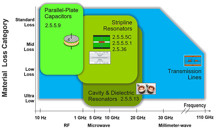
A simple heuristic is to rule out methods that don’t correlate to your frequency of interest. To me, that takes method 2.5.5.9 off the table immediately. The fact that it’s easy to do is perhaps the only reason it’s still in use. That leaves a handful of remaining methods for consideration, including three IPC-TM-650 stripline test methods: 2.5.5.5C, 2.5.5.5.1 and 2.5.36. Properly calibrated, each of the stripline methods is capable of accurate results within their target frequency ranges. A concern remains, however, when comparing one vendor’s 2.5.5.5C data to another’s 2.5.36 data. That’s not to say either method is inaccurate. They’re just slightly different methods. Moreover, there’s a degree of customization that’s left to individual test labs. At best, they represent partially-standard standards.
IPC-TM-650, method 2.5.5.13, anisotropy, and e-field orientation. Electric fields on a PCB are oriented normal to signal-transmission lines, shown by the blue field lines in the stripline cross section in FIGURE 2. Note the heaviest concentration of E-field lines is oriented in the z-direction, or “out-of-plane.” Because of this, Don DeGroot and I recommended in our “Apples-to-Apples Laminate Characterization” paper at DesignCon this year that dielectric measurements for signal integrity applications should be performed out-of-plane. (Feel free to reach out via email to be invited to a webinar on this topic.)
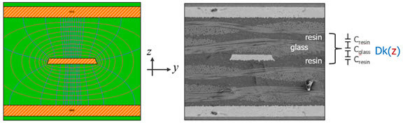
As the figure shows in the microsection on the right, PCB laminates are comprised of a sequentially layered mixture of glass and resin. For this reason, we referred to glass-reinforced epoxy laminates as being “anisotropic.” From a high-speed signal’s point of view, the resin and glass layers look like a series combination of the capacitances of each, resulting in Dk(z), as shown in the figure. This is ideally what we want to measure.
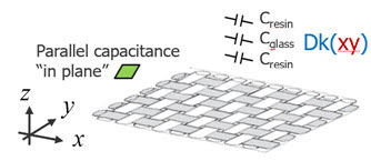
Most methods shown in Figure 1 employ electric fields normal to the material sample (“out-of-plane”), while the Split-Cylinder Resonator method (IPC-TM-650, 2.5.5.13) used by at least seven laminate manufacturers for their Dk/Df dielectric tables use E-fields tangential to the x-y plane of the laminate (“in plane”), as shown in FIGURE 3. These in-plane dielectric-characterization methods analyze the capacitance of resin and glass elements in parallel (rather than series), resulting in Dk(xy) and Df(xy), rather than Dk(z). This would be fine in an isotropic medium, but not anisotropic.
Parting thoughts. While it’s certainly possible to accurately characterize a laminate using 2.5.5.13, it’s like giving someone your waist size when they ask for your height. If I could wave a wand and change the world, I would probably retire 2.5.5.9 and 2.5.5.13 for the reasons noted above. Perhaps in a future column, I’ll go into more detail on the relative benefits of the remaining alternatives.
In closing, I want to make a general point about “standardization” at a conceptual level. If a standard is published and few are employing it, or those who follow it do so in a nonstandard or uncontrolled way, is it really a standard? That’s a discussion, perhaps, for another day.
Au.: Portions of this column were drawn from Don DeGroot, Ph.D., and Bill Hargin, “Apples-to-Apples Laminate Characterization,” DesignCon, January 2019.