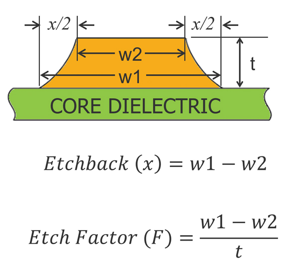
Etch Effects Explained
The impedance implications of the trapezoidal trace.
UNTIL RECENTLY I thought those who believed in rectangular traces were about as common as those who believe in square waves and a flat earth. Recently, though, I came to realize it’s not as clear as I thought, not only for newbies but in general. Over the past 25 years, I’ve acquired a good number of books on PCB design and signal integrity, and you wouldn’t know from reading most of the industry literature that traces were anything but rectangular. Interesting, right?
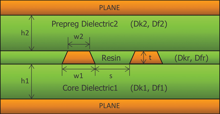
If you’ve read previous “Material Matters” columns, you may recognize the following cross-section from our Z-solver software. Among other things, it shows that the base of a trace, facing the core dielectric, is wider than the side of the trace that faces the prepreg. As such, the trace trapezoids face both up and down in a multilayer stackup. There’s no relationship to the layer number or whether the trace is on the top or bottom half of the board. For this reason, some including me – but not everyone – avoid using terms like “top” or “bottom” with regard to trapezoidal traces.
In the dimensions shown in FIGURE 1, the w1 value at the base of the trapezoid is the value hardware teams and fabricators exchange when talking about trace widths and spacing(s). It’s important to know that actual fabricated boards won’t have quite that much copper. As traces are etched from top to bottom, the etching chemical (“etchant”) remains in contact with the prepreg side of the trace longer than the core side. This makes the prepreg side of the trace narrower than the core side and gives the trace a trapezoidal cross-section. In this column we’ll discuss the reasons for this fabrication phenomenon and the implications for impedance.
Innerlayer etching. Etching innerlayers involves cleaning the copper on both sides of the laminate, applying a photoresist, exposing the photoresist to create the innerlayer pattern, developing the resist, etching away the unwanted copper, and removing the etch resist. This process is automated in most shops, and the chemistry is automatically monitored. As a result, the accuracy and repeatability is quite good. Using this process, it is possible to etch innerlayer traces to an accuracy of ±0.5 mils. This accuracy control helps keep impedance within the tolerances required for transmission lines.
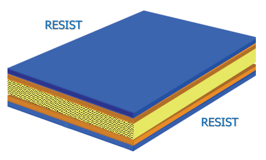
After cores are cleaned, FIGURE 2 shows a blue light-sensitive film or photoimageable “resist” that is applied by heat and pressure to the metal surfaces of the core. The film is sensitive to ultraviolet light. If you ever tour a fab shop, the room where photoresist is handled uses “yellow light” to prevent inadvertent exposure of the resist. The filters remove the wavelength of light that would affect the resist coating.
The Gerber, IPC-2581 or ODB++ data for the part are used to plot film that depicts the traces and pads of the board design. The phototools or artwork include the copper features. This film is used to place an image on the resist.
Innerlayer film is a “negative” image of the copper features, meaning the copper patterns left behind after processing the core correspond to the transparent areas on the film. Core panels are exposed to high-intensity UV light that serves to harden or “polymerize” the film resist, creating an image of the circuit pattern, similar to a slide-negative and a photograph.
The exposed core is then processed through a chemical “developer” that removes the resist from areas that were not hardened by the UV light. Next, the copper is chemically etched from the core in all areas not covered by the remaining blue dry-film resist. After etching, the developed dry-film resist is chemically removed from the panel, leaving just the copper features exposed on the panel.
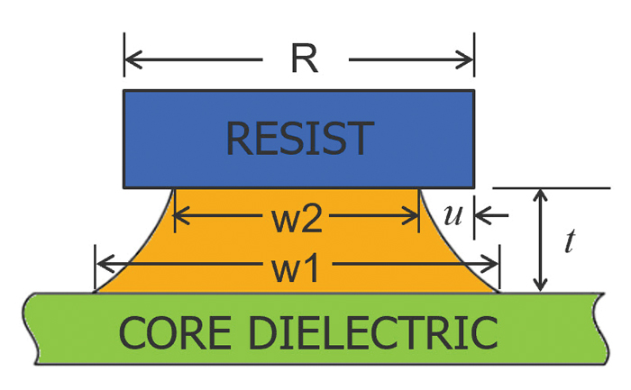
It’s even more nuanced than we’ve alluded to so far. As FIGURE 3 shows, the actual sides of a trace are curved, and an etching “undercut” is below the blue resist. Remember w1 is the dimension hardware teams and fabricators use to describe trace widths. R is the width of the resist the fabricator uses. And the ledge under the resist is the undercut, u. Ideally, R, w2 and w1 are equal. The closer a fabricator can get to this, the better, and good fabricators work hard to achieve this.
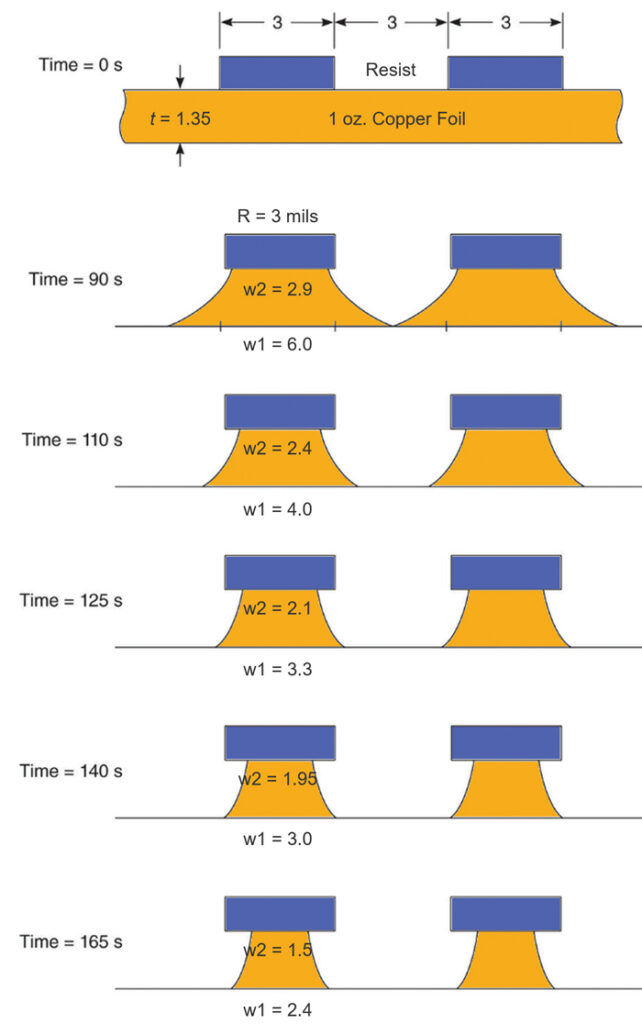
The gap between resist areas is removed evenly at first and then in a progressively cup-shaped fashion until the center area between traces is broken through to the exposed core dielectric, which opens progressively as the etchant goes to work in and under the resist as the side wall is gradually removed through increased exposure. The amount of time the copper is exposed to the etchant determines the final shape of the copper features, as illustrated in FIGURE 4.
A resist width (R) equal to the base of the trapezoid (w1) is ideal etching. In Figure 4, this corresponds to the 140 sec. etching scenario. Note too that if R is less than w1, as in the cases up to 125 sec., the copper features or traces are underetched. In the case where the copper is exposed to the etchant for 165 sec., the copper is overetched. The times here are for this specific example, where cupric chloride was used as an etchant, targeting 3.0-mil line and space patterns, using 1.0-mil resist on 1-oz (1.35-mil) copper foil.
Etch factor. From the parameters in Figure 3, there are two descriptive measures of the etching process: undercutting and etch factor. Undercutting is well-defined. It’s the average overhang of resist after top width reduction. Hardware teams don’t really need to worry about the width of the resist, but the “undercut” term and concept are useful. Obviously, the goal is to minimize the u parameter.

“Etch factor” is quite a bit murkier. Some define it as being proportional to copper thickness, t, and inversely related to the difference between w1 and w2, the width difference in the trapezoid. But depending on whom you talk to, these relationships may be inverted or use different parameters.
I find the relationship shown in FIGURE 5 intuitive. It would be nice if we could agree on a definition like this, where x (“etchback”) is the difference between w1 and w2, and “etch factor” is defined as the degree of etchback per thickness.
Fabricator data. Average suppliers typically maintain roughly 0.25 mils of etchback for 0.5-oz. copper and 0.5 mils of etchback for 1-oz. copper, respectively. Advanced PCB manufacturers can bring these numbers to 0.17 mils for 0.5-oz. copper and 0.45 mils for 1-oz. copper.
I could be talked into changing the practice, but to avoid getting the complications of conflicting definitions, I’ve worked in percentages, specifically the ratio between w2 and w1 (with the goal to get as close as possible to 1.0).
Using this approach, advanced PCB manufacturers might achieve w2/w1 of 0.972, for example, for 0.5-oz. copper. Similarly, research shows advanced manufacturers can achieve w2/w1 of 0.925. The limitation with this approach is that it presumes a specific value for w1: in this case, 6 mils.
Plated layers. I hate to open another can of worms to discuss outer layers but will touch on the subject for completeness. In short, outer layers are even more complicated, particularly in the case of multiple plating steps and when copper reduction techniques are used to keep the surface copper thickness down. Sometimes, microstrip traces are anvil-shaped rather than trapezoidal-shaped, but more commonly they look more like a “mesa,” borrowing a term from geology, with the top-plated section almost vertical and the trapezoidal cross-section at the bottom; i.e., a rectangle on top of a trapezoid, with the rectangle representing the plated Cu. To model this, some use a 1-mil etchback for a plated microstrip. This seems to best represent “most” outer layers, although it is still incorrectly modeling the cross-section as a trapezoid.
Plated layers often have “other challenges,” including that there may be one, two, or even three plating passes. Some designs are plated 1x and end up exactly 1-mil thick, while other boards have 1x plating and are considerably thicker.
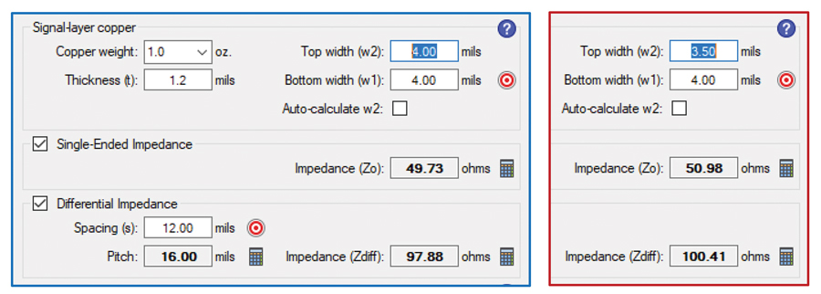
Impedance implications. Let’s consider an “average” PCB fabricator, where a 1-oz. stripline layer has 0.5 mils of etchback, and compare the impedance results against a trace where etchback is ignored. In FIGURE 6, the left image with the blue border assumes a rectangular trace cross-section. The image on the right includes the 0.5 mils of etchback for a single-ended transmission line targeting 50Ω and a differential pair targeting 100Ω. As you can see, the single-ended impedance difference is 1.25Ω and the differential-impedance difference is about 2.5Ω. Could your design live with such a difference? It depends on a lot of factors, some that you control and some random. You don’t directly control Dk variation or copper-thickness variation from nominal, for example, but you can specify impedance at +/-10%. The difference we’re showing here would be stacked on top of Dk variation, copper-thickness variation, and any other variation in fabrication. In short, you’re giving up ohms right out of the gate, which is not good design practice.BIBLIOGRAPHY
- Gareth Parry, “Etching Process and Technologies,” Printed Circuits Handbook, seventh edition, Chapter 37, McGraw-Hill Education, Clyde Coombs and Happy Holden, ed., 2016.
- Siemens, HyperLynx SI/PI User Guide VX.2.8, 2020.
- Lee Ritchey, Right the First Time, vol. 1, 2003.