Preparing for Next-Gen Loss Requirements – Part 1
Can signal-integrity test vehicle results be accurately simulated?
Ed.: This is Part 1 of a three-part series on preparing for next-generation loss requirements.
There are a lot of factors to juggle to stay on top of the parameters that contribute to loss. Frequency, copper weight, resin system, glass characteristics, dielectric thickness, trace width, copper roughness, and fabricator processing all contribute to the discussion if you’re savvy and driving fast, with both eyes open.
If frequencies aren’t increasing, no need to worry. But if your windows are getting chopped in half year-over-year, read on.
Background. Several years ago, I marketed laminates for servers. Older generations bumped up frequencies incrementally, but then we ended up dealing with frequencies that doubled from one generation to another, with downward pressure on costs.
There are multiple server platforms, of course, but a quick review of Intel’s PCIexpress (PCIe) trends shows performance jumps going from 8Gbps (4GHz) to 16Gbps (8GHz) to 32Gbps (16GHz) with PCIe 5.0. Those are incredible jumps, particularly when also trying to hold down material costs. The world would be easier if no one had to pay for the performance improvement, but loss and cost are intimately intertwined. And it’s not just Intel and PCIe. Multiple interconnect standards have transitioned from incremental speed increases to doubling generation-over-generation.
To accommodate, it’s common in the server world to build test boards with defined geometries, tracking all the relevant parameters noted above across multiple laminate vendors, resin systems and fabricators, but the process of doing so takes about six months from concept to completion. In today’s design environment, who can wait that long? A lot of designers, I would expect, don’t have the luxury of long server-ecosystem lead times, where the entire system architecture is the long pole in the project schedule tent.
For the purpose of reeling in schedules and narrowing the solution space, I’ve been focused on developing tools that make tradeoffs early in the system-design process, including frequency, interconnect loss budgets, and the design knobs that designers control, including resin system, cost, copper roughness and trace length.
My big question. My BIG QUESTION, which I don’t fully know the answer to before simulating, is whether I could have predicted what I already know from SITVs (signal-integrity test vehicles), based on frequency, resin-system properties, copper characteristics, etc.
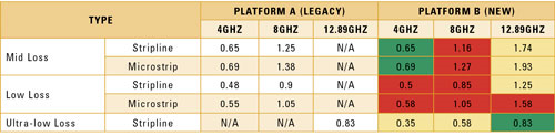
I know before performing any simulations what products were successful meeting the loss requirements in TABLE 1, but my interest is actually knowing whether simulation would have provided assistance toward predicting the outcome.
SITVs are designed to emulate typical design configurations, while isolating the relative performance of 3- and 4-mil cores, both in microstrip and stripline configurations, using the same test vehicles (TVs). For simplicity, this column focuses on striplines, but the same process applies to microstrip-signal requirements.
Backwards engineering platform A (legacy). Platform A had an insertion-loss requirement of 0.48dB/inch for the platform’s low-loss boards. Built into this target, of course, are typical interconnect lengths for the platform. Test vehicles for many different competitive mid-to-standard-loss laminate systems were created across multiple PCB fabricators, to find the sweet spot for cost and loss. If you have a lot of money and time, that’s certainly one way to do it.
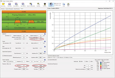
My first objective, using the specified SITV cross-section, was to determine which Df characteristics would be required to meet the insertion loss (IL) goal. FIGURE 1 shows that at 4GHz a laminate with a loss tangent of 0.013 would meet the 0.48DB/in. target with a little margin. This Df number was determined by entering all the SITV cross-section data, including the Dk from one of the materials under consideration, along with copper roughness, and then determining what Df value met the IL threshold. This is helpful going in. We’re looking for resin systems with actual Dfs at 0.13 or slightly lower.
My second objective was to take one of the laminate systems that was successful on Platform A, with known IL test results, to see whether vendor-published Df numbers would produce the same insertion loss. The vendor-published Df for Laminate A was 0.008 at 4GHz. For this material and the construction shown, the simulated IL using the published Df was fine, but measured insertion loss was just beyond the 0.48dB/in. low-loss requirement at 0.485dB/in., which tells us the actual Df may be a good bit closer to 0.013 at 8GHz. Toward that end, the test vehicles indeed taught us something. As I recall, the laminate in question was bumped down to the mid-loss applications, while slightly more expensive materials were used for the low-loss applications.
This wasn’t a super-high-tech laminate, but the process certainly scales to higher speeds, as we will see below.
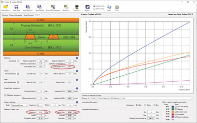
Low-loss requirements at 8GHz. Platform B (new) shows a low-loss IL (8GHz) requirement of 0.85dB/in. for a stripline. This guideline is based on typical interconnect lengths for the platform, frequency and the receiver’s tolerance for loss. Using the same SITV cross-section noted above and Dk/Df values from one of the vendor materials proposed for this application, Laminate B, we can see in FIGURE 2 that the laminate-vendor-published Df at 0.007, along with other factors such as the Rz=1.3µm copper roughness, resulted in an insertion loss of 0.60dB/in. This is more than enough margin against the 0.85dB/in. target, which is a good thing. However, in hindsight, the SITV-measured insertion loss was 0.645dB/in., meaning the actual Df was a little bit higher. Trial-and-error with the field solver reveals a Df (8GHz) of 0.008 may be more realistic for this particular laminate. Simulation also showed a Df of roughly 0.013 was needed to meet the IL target at 8GHz.
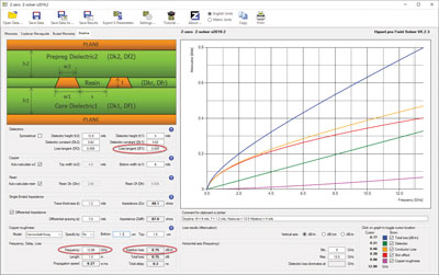
Low-loss requirements at 12.89GHz. The process is similar but gets more expensive at higher frequencies, requiring we work with sharp pencils. 12.89GHz is the PAM4 Nyquist frequency for a 100 Gbps signal. I like to start these simulations with a material that’s been proposed for this space, so I’ll change the Dk and Df accordingly as a starting point, modeling Laminate C. FIGURE 3 shows the results, with a vendor-published 0.005 Df at 10GHz. The 0.74dB/in. result, using 1.1µm copper (Rz), is well within the 1.25dB/in. low-loss target, but this is just a first pass with datasheet Df numbers. To meet the requirement for a 12.89GHz Platform B signal, simulation shows we need a 0.013 Df (12.89GHz) material.
Using hindsight, we’re able to backwards-engineer the effective Df from actual, fabricated SITVs. Of course, we wouldn’t typically have the IL loss in the planning phase when we’re selecting materials, unless the PCB fabricator had collected it for another project as part of its laminate offering. Our main purpose here, however, is to guide how we may need to interpret vendor Df numbers when framing the solution space for a new platform. The fabricated SITV’s measured IL loss was 0.684dB/in. for this configuration. In this case, we learned vicariously that the published Df number for this material was reasonably accurate. We also learned Laminate C, a PPE resin system at more than two times the price of the next step down, was overkill for the low-loss target. The good news is we’ve found a potential material for the ultra-low-loss boards. The question becomes whether we can stretch the lower-priced Laminate B discussed in the 8GHz section to cover this application, and that’s exactly what happened in practice.
Keep in mind we’re now talking about 12.89GHz. It’s a completely different league than the 4GHz we started with, and that’s a key point in this column.
Conclusion. The point here was to demonstrate a methodology by which a PCB fabricator, design team or laminate vendor could convert interconnect loss requirements into Df requirements and project a material’s insertion-loss performance, without spending several months – from laminate production to PCB fabrication to testing – making SITVs. Doing so without spending tens of thousands of dollars and months of waiting for SITVs is a big benefit. Which makes the most sense: spending $100,000 and waiting six months for answers, or spending a fraction of that and simulating what to expect prior to SITV fabrication?
Along the way, we see sometimes vendor Df numbers a good bit higher in practice than the published vendor value, in some cases by as much as 0.004. With this word of caution, it’s helpful to know a good 2-D field solver can be employed at any point in the design cycle without going to the trouble of building and testing test vehicles.
In Part 2 of this series, I’ll outline the means by which insertion-loss requirements are determined. In Part 3, I’ll suggest a better method for obtaining more accurate Df numbers without building test boards.