Preparing for Next-Gen Loss Requirements, Part 2
Can signal-integrity test vehicle results be accurately simulated?
Ed.: This is Part 2 of a three-part series on preparing for next-generation loss requirements.
Here in Part 2 of the series, I’ll outline the means by which insertion-loss requirements are determined. In Part 3, I’ll suggest a better method for obtaining more accurate Df numbers without having to go to the trouble of building test boards.
As I stated in last month’s column, if you want to stay on top of the parameters that contribute to loss, there are a lot of factors to juggle. Frequency, copper weight, resin system, glass characteristics, dielectric thickness, trace width, copper roughness, and fabricator processing all contribute to the discussion if you’re savvy, driving fast, with both eyes open.
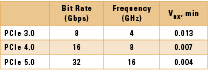
Component manufacturers will typically specify a loss budget for a chipset. There are multiple server platforms, of course, but Intel’s PCI Express (PCIe) trends provide a good example of the performance jumps seen across today’s interconnect standards. TABLE 1 shows how PCIe speeds have changed in recent years, from PCIe 3.0 to PCIe 5.0.
It is also possible to derive the budget. The relationship for estimating an interconnect loss budget is:
Attenuation budget (dB) = 20 x log (VRX, min / VTX, min)
This loss figure reveals attenuation requirements before employing pre-emphasis or equalization.
Some signal integrity software solutions include these guidelines, represented as eye masks, defining minimum and maximum “keep-out regions” for received signals. At a glance, an eye mask will show if an interconnect is acceptable from a signal-quality standpoint across many bit transitions. FIGURE 1 shows a PCI Express Gen 5.0 eye mask from Mentor’s HyperLynx software. It’s important to observe the inner keep-out region, represented by Top Min in the figure, correlates to the VRX, min column in Table 1. From PCIe 3.0 to 5.0, these requirements have narrowed significantly.
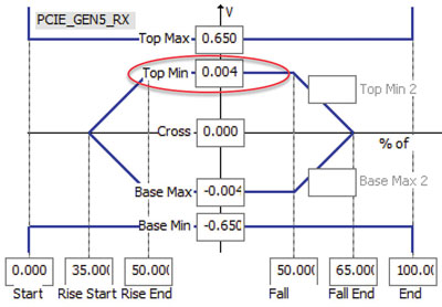
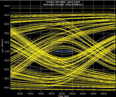
FIGURE 2 shows simulation results for an 8 Gbps signal over a 24″ transmission line using a material that was successful on platforms that used PCIe 3.0. The loss tangent or Df for this material is 0.012. The blue keep-out region doesn’t have any bits encroaching on it, which is what we want. Obviously vias, connectors and copper roughness come into play as well. This is simply intended as a high-level example of the interplay between frequency, the eye mask, and the eye diagram. Increase Df above 0.012 and bits begin encroaching on the eye mask’s inner keep-out region.
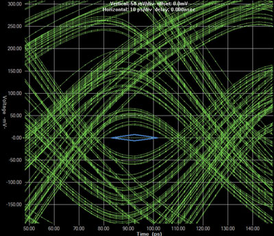
Keeping with this theme, let’s consider a more expensive, lower-loss material for the next-generation requirement. We’ll use 16 Gbps and the PCIe 4.0 eye mask, both corresponding to Table 1. To make this work, I used a material with a Df of 0.008, and I had to change the transmission-line length to 15″, which was right on the edge of what would work. The additional factors noted above must also be considered, but we’ve learned a few things that get us in the ballpark from a dielectric-selection standpoint. FIGURE 3 shows the result. Note the vertical scale was changed, adapting to the tighter keep-out requirements with PCIe 4.0 versus those of 3.0. The same simulation exercise could be performed for PCIe 5.0 and higher frequencies, although the task of producing acceptable eye patterns at the receiver gets much tougher.
In Part 3 of this series, I’ll suggest a better method for obtaining more accurate Df numbers without having to go to the trouble of building test boards.