The No. 1 Weapon Against Crosstalk
Trace separation; length parallelism; stackup: Does one stand out?
It’s been some time since I’ve seen an article on crosstalk, so I decided to take the opportunity to walk through the subject in a soup-to-nuts overview for those in the PCB design community who may be interested in why crosstalk-savvy PCB designers and hardware engineers use various design rules for controlling crosstalk. In the process of doing so, we’ll identify which design tweaks provide the most leverage for controlling far-end crosstalk.
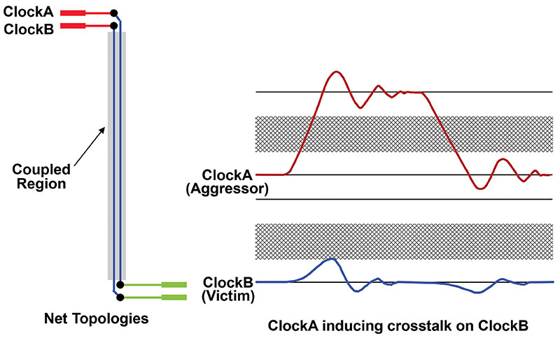
Crosstalk is unwanted noise generated between signals. It occurs when two or more nets on a PCB are coupled to each other electromagnetically, (even though conductively they are not connected at all). Such coupling can arise any time two nets run next to each other for any significant length. When a signal is driven on one of the lines, the electric and magnetic fields it generates cause an unexpected signal to also appear on the nearby line, as shown in FIGURE 1.
A number of factors combine to create an unwanted crosstalk signal: the length over which the traces are coupled, the distance between the traces, their positions in the PCB stackup, what driver ICs are used on both the “aggressor” and the “victim” lines, whether the lines are terminated, and so forth.
Crosstalk is a particularly hard phenomenon to anticipate and control unless it is simulated, because there is almost no way of intuitively knowing how much crosstalk voltage and current will develop due to a given coupling. Nevertheless, semi-conservative design guidelines can be useful, although almost always at the expense of board real estate.
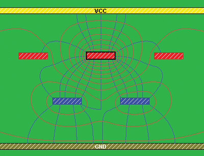
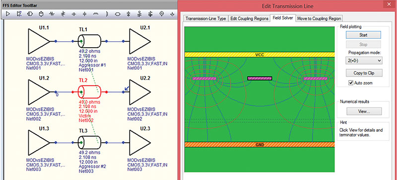
In crosstalk parlance, the “aggressor” signal or trace switches and causes crosstalk. The “victim” signal or trace responds by developing an unintended signal. The effect is three-dimensional in nature. Victims can be adjacent on the same layer or above or below the aggressor (FIGURE 2).
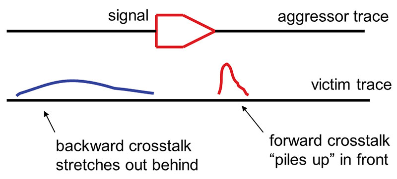
Actually, two coupled signals are imposed upon the victim net: a forward signal and a backward signal. The “forward” pulse travels along with the aggressor’s signal, and a “backward” pulse travels back from the aggressor signal. Crosstalk at the victim’s far end is called “far-end crosstalk,” or FEXT, and coupled voltage at the near end is called “near-end crosstalk” (NEXT). FIGURE 3 shows both forward and backward crosstalk. The backward signal often ends up traveling forward after reflecting off a driver.
Current is injected into the victim by electric fields (the lines that run orthogonal to the traces in Figure 2) caused by capacitive coupling interactions between the aggressor and victim nets. These interactions are affected by conductor surface area and distance, and generally terminate at adjacent conductors. Voltage is induced on the victim by magnetic fields. These are inductive (transformer) coupling interactions, which are somewhat circular – surrounding the aggressor and victim nets. These interactions are not generally stopped by conductors and can therefore extend around multiple adjacent conductors.
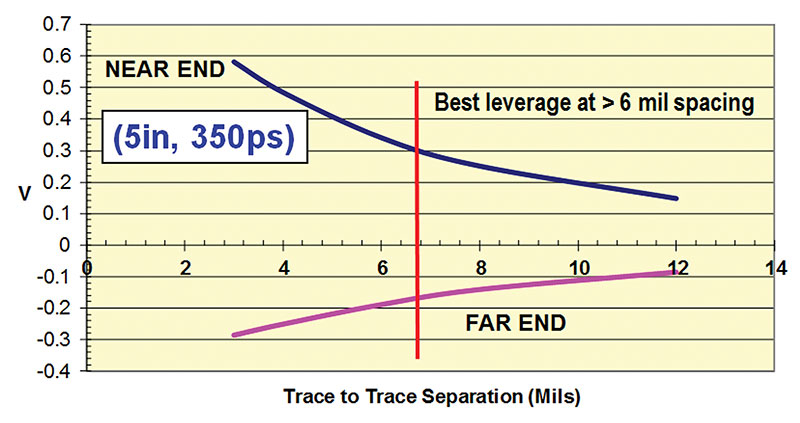
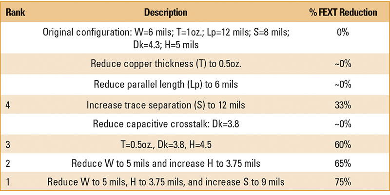
Crosstalk guidelines. The most common crosstalk design rules involve trace-to-trace separation. A PCB designer might, for example, set an auto-router to 4-mil trace width and 4-mil spacing. This will, of course, maximize router completion, but the resulting design will incur 20 to 60mV of crosstalk. Adjusting noise-sensitive victims to more than 6-mil trace-to-trace spacing can help avoid this problem (FIGURE 4).
Because electric fields terminate at reference planes, traces close to reference planes have reduced crosstalk. Capacitive trace-to-trace coupling drops off quadratically with the distance from the reference plane(s), so traces within 4 mils of a reference plane will be much more immune to crosstalk than a trace 6 or more mils from the nearest reference plane. And symmetric striplines – because of their relative proximity to not one, but two reference planes – have relatively higher immunity than microstrip signals.
Moreover, there’s a dielectric-constant effect to consider. High dielectric constants (Dk) concentrate the electric field, resulting in relatively poorer crosstalk performance, in a roughly linear relationship between Dk and capacitive crosstalk.
Example: Crosstalk on a bus. Suppose you’re designing a bus and want to guarantee no more than 200mV of crosstalk can occur on any signal. Here is the process of developing the proper routing constraints to achieve it. A typical bus in a modern digital system contains many physically parallel traces – 16, 32, 64 – maybe even more signals. To analyze crosstalk on such a bus, however, you can narrow the scope to a single “victim” trace, with “aggressor” nets on either side.
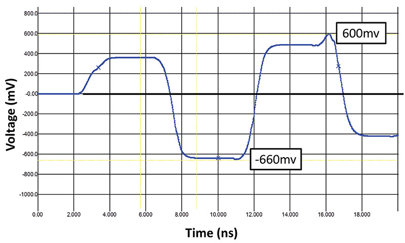
Let’s start with coupled, coplanar 6.0-mil-wide (W) striplines, running parallel for 12″ with trace-to-trace separation of 8.0 mils (S), through a 4.3 Dk dielectric with a 5.0 mil height (H) (FIGURE 5). A simulation with HyperLynx LineSim (FIGURE 6) shows the far-end crosstalk to see how much crosstalk occurs with the initial arrangement. With 590ps (0.59ns) driver-switching speeds on the two aggressor nets, and no signal injected on the victim net, about 600mV on the positive side will be injected into the far-end victim waveform, and 660mV on the negative side – both well beyond our design criteria of 200mV maximum crosstalk.
Crosstalk is a complex effect influenced by many different geometric factors: e.g., driver-IC technology (Tr, Tf, output impedance, and drive strength), trace width (W), copper weight (T), parallel-line length (Lp), trace separation (S), PCB stackup [layer ordering, Dk, and dielectric thickness (H)], and line-end termination. (Crosstalk generally requires more complex termination than single-line reflections.) Rules-of-thumb exist for controlling crosstalk, but to minimize crosstalk while controlling cost on a specific design requires a good simulation tool. In the following section, we’ll go through an iterative process for dealing with crosstalk on the design in Figures 5 and 6 to see if some reasonable design rules emerge.
Crosstalk reduction techniques. A crosstalk lever that might be overlooked sometimes is the copper thickness. In the example above, signals have used 1-oz. copper. That’s thick for a signal trace. One might think reducing copper thickness will reduce capacitive coupling, though simulation shows the result is not significant in practice. Nevertheless, for the remainder of this discussion, we’ll use the more common 0.5-oz. copper.
One possible technique for reducing crosstalk is to reduce the length over which aggressors and victims run parallel to one another. This poses some practical problems on the routing side – those traces are parallel on a board for a reason – but it’s instructive to see what happens when the parallel coupling region is reduced from 12.0″ to 6.0″. Surprisingly, this doesn’t reduce crosstalk at all; it simply moves peak crosstalk amplitudes to the left in the time domain. Reducing parallelism alone, as a crosstalk lever, isn’t quite as powerful as we might think.
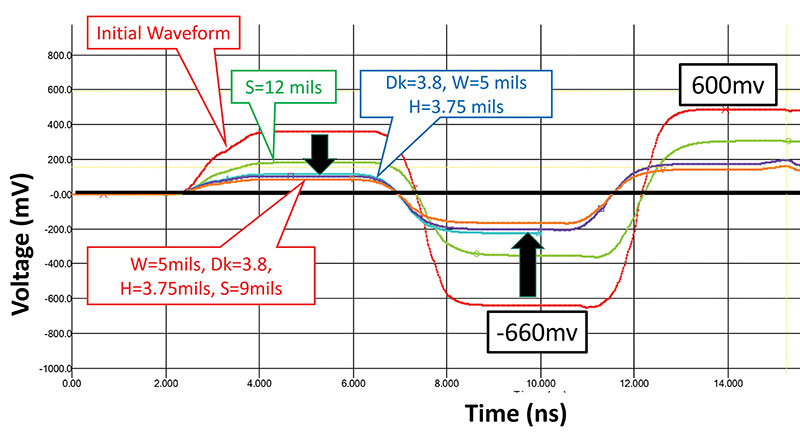
Another common way to decrease the crosstalk is to increase the separation, S, between the traces. Increasing trace separation from 8 to 12 mils reduces crosstalk to 400mV on the positive side, and -400mV on the negative side – still well beyond where we would like, and in the process of making this change, we use a good bit more board space.
There are many ways besides trace separation and length parallelism to affect crosstalk. One that is sometimes overlooked is the PCB stackup. Recall we started with Dk=4.3. What happens if we try to reduce capacitive crosstalk by using a lower-Dk material, say D=3.8? Through simulation, it turns out the improvement from this change alone is negligible. In the process of using 0.5-oz. copper, and reducing the Dk of the dielectric, however, trace impedance increased from roughly 50Ω to just under 57Ω. (Remember: Impedance is inversely related to the square root of trace capacitance, which is tied to the Dk of the dielectric.) So, reducing the dielectric thickness (H) from 5.0 mils to 4.5 mils between the stripline layer of interest and the nearest reference plane increases the capacitance again, pulling the impedance back to around 50Ω. The combination of these factors gets us much closer to our goal, resulting in 211mV on the positive side down to about 230 mV on the negative side – more than 60% but still above our target of 200mV.
Reducing trace width (W), which increases impedance (Z0), and then narrowing the dielectric thickness (H) to pull the impedance back down to around 50Ω is another potential way to reduce crosstalk. Reducing W to 5.0 mils and H to 3.75 mils results in roughly 200mV of both positive and negative crosstalk.
By narrowing trace width (W) by 1.0 mil, the overall bus width decreased in mils by the number of bits minus one. With an interest in gaining more margin, while keeping the overall bus width as in the initial design, adding another mil to the spacing (i.e., taking S from 8.0 to 9.0 mils) results in plenty of margin: 160mV on the positive side and 170mV on the negative side.
TABLE 1 summarizes effects on the topology in Figure 5, and their relative impact on FEXT, ranked by relative reduction in worst-case crosstalk.
Parting thoughts. As I’ve been trotting around talking to engineers and PCB designers for the past 10 years, I’ve heard many references to the use of thinner dielectrics, so for some readers the contents of this article may be review. But I have yet to see an article that compares the different levers for controlling crosstalk, with emphasis on the fact that material selection and specifically laminate thickness play the most pivotal role in controlling far-end crosstalk (FEXT).
In a future column, I’ll expand on the details of how tighter E-field coupling to the nearest reference plane works, with some accompanying visuals and perhaps a review of Maxwell’s equations.
References
1. Bill Hargin, Printed Circuits Handbook, seventh edition, McGraw-Hill Education, chapter 20, 2016.