What Surrounds a Typical Trace?
At higher speeds, the micro-environment around traces can alter simulation results.
In the past few weeks, e-mails from multiple sources crossed my inbox asking about the relationship between epoxy resin and signal behavior. With a couple of SI guys on one side and a career PCB manufacturing guy on the other side hitting me the same week with different versions of the same question, I thought it would make for an interesting column topic.
FIGURE 1 shows the initial image I was provided, along with the question what surrounds a typical trace? At face value, this may sound trivial, but it’s a reasonable issue for a signal-integrity practitioner to be concerned about.
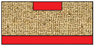
FIGURE 1. This started as a microstrip representation, but it’s more representative of a stripline.
The answer depends on what’s above the signal layer, what’s below it, and where it appears in the stackup. Figure 1 is a reasonable representation of an inner stripline layer, if the cross-hatched dielectric representation is a prepreg with a fully cured core above it. In this case, the copper features on the signal layer are encompassed by a layer of resin that comes from the adjacent prepreg, as a result of heat and pressure applied during the lamination process.
After making the above observation, I learned that the trace whose surroundings were in question was on an outer microstrip layer, with air on top. In this case, the cross-hatched area would typically be prepreg as before, but Figure 1 no longer accurately represents the “micro-environment” around the trace. The reason outerlayer copper features aren’t surrounded by resin is that the entire printed circuit board sandwich goes through the lamination press with a solid piece of copper on top. None of the resin flows around the trace, because the resin is fully cured before features in the outerlayer copper are etched. From there, drilling and plating take place, and solder mask is typically applied. As a result, a more accurate model of the micro-environment around the trace would either be air or solder mask, as shown in FIGURE 2. This is significantly different from Figure 1, of course, and we should expect different results in both simulated and manufactured circuit boards.
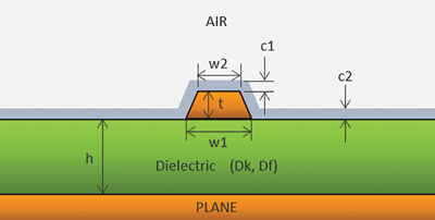
FIGURE 2. A more accurate representation of the microstrip trace in Figure 1, including conformal coating (solder mask).
So what? At this point, you may be asking, “Who cares?” And if you’re signaling at 1MHz, you probably don’t care. But if you’re pushing multi-gigabit speeds, knowing the “micro-environment” around the signals you are modeling with that expensive SI software might be a good idea, right? A more accurate picture of Figure 1, if it represents a stripline, is shown in FIGURE 3.
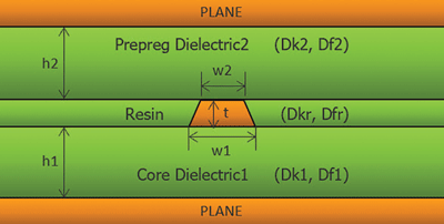
FIGURE 3. A more accurate representation of the cross-section in Figure 1, if it represents a stripline.
The figure shows innerlayer (stripline) signal layers are surrounded by resin on both sides. This is important because the resin has fundamentally different electrical properties than the adjacent prepreg or core materials.
It’s important to realize that core and prepreg spec sheets report composite dielectric constant (Dk) and dissipation factor (Df) numbers for the glass and resin combined. No surprise there, but these composite Dk and Df values represent highly dissimilar components. Electrical-grade glass fiber (“E” glass), for example, has a Dk of roughly 6.8. While it depends on the resin system – there are at least 100 to choose from – typical epoxy resins are in the ~3.0 Dk range. Lower Dks mean higher signal-propagation velocities and higher impedances. It’s reasonable to ask how significant this effect is, so that’s what we’ll investigate next.
Electrical impacts from stackup parameters.
Some SI practitioners assume the dielectric adjacent to and on the same plane as the signal are represented by the electrical parameters of the vertically adjacent laminate (core) or prepreg, so we’ll start with this notion as a baseline, while looking at impedance, propagation speed, and predicted insertion loss as dependent variables for comparison.
We’ll use 0.5oz. copper, a 6-mil wide stripline trace, 5-mil thick core and prepreg, a Dk of 3.85, with Df equal to 0.010. Using the dielectric-property assumptions noted in the previous paragraph, the resin adjacent to the signal layer will be modeled with the aforementioned parameters.
Temporarily ignoring copper roughness and etch effects – topics for another day, perhaps – the stripline in Figure 2 results in a 43.8Ω impedance, a propagation velocity of 6.02in/ns, and a simulated insertion loss of 0.81dB/in at 10GHz.
Next, let’s look at the same cross-section, while including adjustments for the fact that resin will surround the signal traces. An algorithm built into industry modeling software estimates “neat” (pure) resin properties from the adjacent prepreg as Dk=3.08 and Df=0.015, resulting in a 44.1Ω impedance, a propagation velocity of 6.06in/ns, and a simulated insertion loss of 0.83dB/in at 10GHz. So, less-accurate modeling of the resin layer leads to underestimation of impedance, propagation velocity and insertion loss. Whether these differences are enough to cause downstream SI problems depends on what is being designed, over what transmission-line lengths, and at what frequencies. FIGURE 4 shows these simulated results in Z-zero Z-solver software.
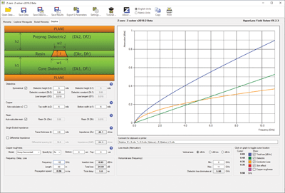
FIGURE 4. A single-ended stripline, including modeling of “neat” resin using Z-zero Z-planner software and Mentor’s HyperLynx field solver.
Microstrip modeling.
Given an ounce of copper plating, the incorrectly drawn microstrip in Figure 1 results in a 54.6Ω impedance, a propagation velocity of 7.2in/ns, and a simulated insertion loss of 0.51dB/in at 10GHz. But it’s an imaginary construction … a GIGO exercise!
Modeling Figure 1 and including solder mask results in a somewhat similar 53.7Ω impedance, a propagation velocity of 6.87in/ns, and a simulated insertion loss of 0.62dB/in at 10GHz. Can you survive overestimating propagation velocity by 0.33in/ns and underestimating insertion loss by 0.11dB/in? Perhaps. The problem multiplies when you consider whether these differences are happening across 5″ to 15″ traces or 30″ to 40″ backplanes and at progressively increasing speeds.
Conclusion.
Differential-signaling characteristics and crosstalk will also be affected by these adjustments to the micro-environment on signal-trace layers. And, as Lee Ritchey often points out, differential signals are comprised of two single-ended transmission lines that may or may not be closely coupled to each other. I decided to focus on single-ended signals to avoid blurring the main point, which is that if you’re signaling at multi-gigabit speeds, details like the micro-environment around traces matter. You can simulate your face off, but absent the correct underlying stackup details, that expensive SI simulator may be providing less-than-accurate results.