Why We Simulate
When I was cutting my teeth in high-speed PCB design some 25 years ago, speeds were slow, layer counts were low, dielectric constants and loss tangents were high, design margins were wide, copper roughness didn’t matter, and glass-weave styles didn’t matter. We called dielectrics “FR-4” and their properties didn’t matter much. A fast PCI bus operated at just 66 MHz.
As speeds increased in the 1990s and beyond, PCB fabricators acquired software tools for designing stackups and dialing in target impedances. In the process, they would acquire PCB laminate libraries, providing proposed stackups to their OEM customers late in the design process, including material thicknesses, copper thickness, dielectric constant, and trace widths—all weeks or months after initial signal-integrity simulation and analysis should have taken place.
Speeds continued to increase in the 2000s; design margins continued to tighten, and OEM engineers began tracking signals in millivolts (mV) and picoseconds (ps). Figure 1 illustrates these trends starting in 2000, emphasizing the trajectory of PCI Express, from PCIe 3.0 in 2010 to PCIe 6.0, which is just on the doorstep.
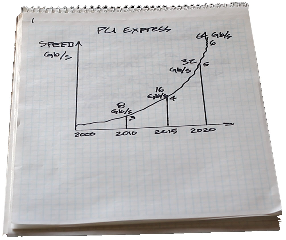
gigabits per second (Gbps) from 2000.
(Artwork by yours truly.)
In webinars and training events I often pose this question: “Why do we simulate?” I ask because the answers tell me a lot about the audience, and some wise older person long ago told me and my fellow students to “always know your audience.”
When I ask that, I get answers like faster signaling speeds, calculating impedance or loss, opening eyes and avoiding inter-symbol interference, controlling crosstalk, etc. These are all good answers, but a bit on the periphery in my view.
One astute signal integrity practitioner offered that we simulate for only two reasons:
1. To make design decisions (i.e., evaluate tradeoffs during design).
2. To verify a design before manufacturing(verification).
The only question that designers really care about is, “Will it work and by how much?” This implies that the simulation should be able to produce tangible metrics that can be related to design success or failure. Fair enough.
This is a good description for “why we simulate,” but so far, I’ve never heard anyone mention the most fundamental reason, in my opinion, for signal integrity (SI) or power integrity (PI) simulation: To predict the negative impact that the physical world has on the electrical world, and to mitigate or prevent the negative effects proactively.
You can have hundreds of thousands of dollars’ worth of VNAs, oscilloscopes, and simulation software, but simulations will be invalid unless you carefully model PCB fabrication details. The bridge between a high-speed design and a high-speed design that works across several fabricators goes through the backbone of the PCB—the stackup—which touches every single high speed signal. My chicken scratch in Figure 2 illustrates this. (Yes, I knowhow to use PowerPoint.)
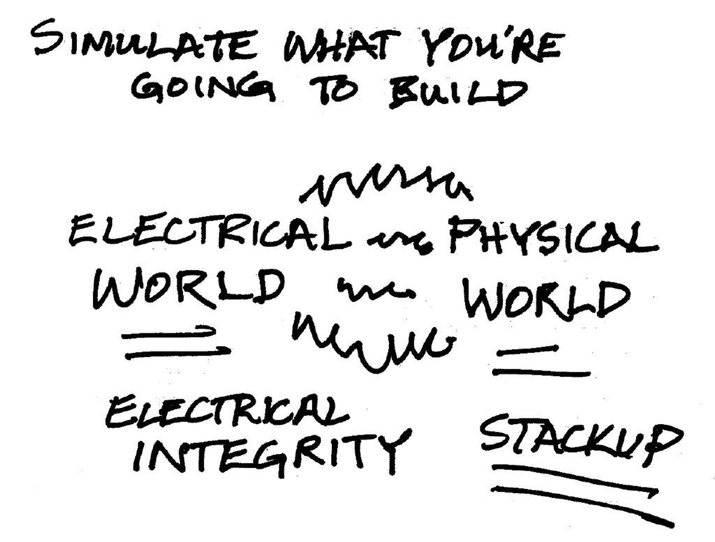
or power-integrity simulation is to predict the
negative impact that the physical world has on the
electrical world, and to mitigate or prevent the negative
effects proactively. (Artwork by yours truly.)
The Progressive Evolution Toward Simulation
Over the years, I’ve tracked five different phases in the evolution toward simulating hardware performance, as illustrated in Figure 3.
To do this, we need to do our best to “simulate what we’re going to build,” as Figure 2 points out. A good simulator accelerates the rate at which you can experiment with alternatives, allowing engineers to optimize not only to signal quality, but also cost tradeoffs.
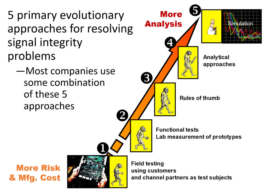
five approaches for resolving signal integrity problems.
But it’s about more than having expensive simulation tools. In my work, quite a number of PCB stackups cross my desk, and depending on who or what tools were involved in a given design, there are manufacturing parameters that affect both impedance and signal loss that many design teams can improve upon. At progressively higher speeds, critical factors for signal integrity now include not only impedance, but loss, copper roughness, and glass-weave skew. Indeed, everything that happens in the process of physically building a PCB affects signal quality in a negative way and the details need to be accounted for across not just one PCB stackup, but across stackups from every PCB fabricator involved with a design.
Factors That Impact Impedance
EDA tools, including those made by my company, can be super useful, if you know what they are really modeling. Even here, the results are only as good as the data being put in. The primary parameters that affect impedance are shown in Table 1, including their relative contributions.
If you work this list from top to bottom, starting with getting a better handle on dielectric thicknesses and working your way down, you’ll be better equipped to dial in your nominal parameters with enough margin to know that you’re not going to fall off the cliff. And yet, every week I see engineering teams straining to perform complex analyses using datasets with questionable merit, and without fully grasping the parameters and priorities (1 through 7) noted above.
For example, I’ve never seen detailed, per layer percent-copper values from actual PCB layouts being used by PCB fabricators to compute pressed prepreg thicknesses. And number 4 in Table 1 can be particularly problematic. I’ve searched far and wide amongst hardware OEMs, PCB manufacturers, and laminate manufacturers, and I would submit that dielectric constants are the least understood parameters in PCB fabrication. Trace width (#5) is closely tied to fabricator etching processes. Studies have shown that average PCB suppliers typically maintain roughly 0.25 mils of etchback for half-ounce copper and 0.5 mils of etchback for 1-oz. copper, respectively. Advanced PCB manufacturers can bring these numbers to 0.17 mils for half-ounce copper and 0.45 mils for 1-ounce copper. Knowing what your fabricator can maintain and modeling it in simulations can increase impedance accuracy by several ohms.
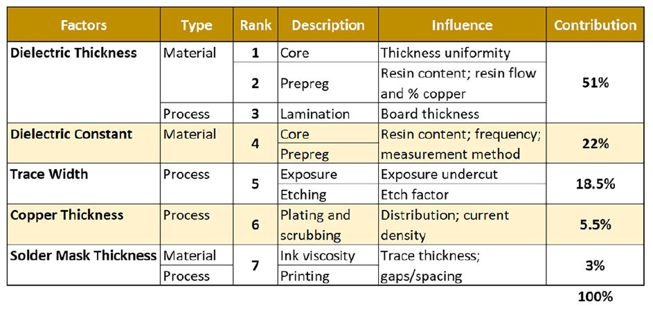
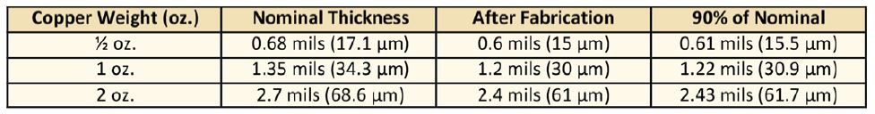
Copper thickness (#6), is another parameter that impacts impedance. I often see engineers, designers, and EDA tools rounding nominal copper thicknesses for half-ounce copper to 0.7 mils (18 μm), 1.4 mils (36 μm), and 2.8 mils (71 μm). I’m not normally against rounding, but when you’re rounding in the wrong direction, it needs to be questioned. Table 2 lists actual thicknesses and conversions.
Board thickness, too, will be affected. On a four-layer design, the difference may not be significant, but on a 20-layer design using one-ounce copper throughout and the wrong assumptions, your board thickness will be off by as much as 4 mils. I’m pretty sure the mechanical engineers, if no one else, would appreciate it if PCB designers worked with a sharper pencil.
Conclusion
Whenever I talk in person with SI consultants— people who do SI consulting for a living—I ask them this question: “Of all the smoke-jumping projects you’ve been brought in for where there were serious SI problems, how many of those projects had stackup issues?”
So far, the only answer I’ve gotten back has been “100%.” All told, the factors I’ve noted that impact impedance can put your designs near the edge of your tolerance targets. So, it’s not just about having an expensive simulator, it’s about feeding it the right parameter values, and that’s much of what I’ve been focused on for the last few years with my company, Z-zero. Shoot me an e-mail if you have any war stories on the subject. I always like hearing from designers on the front lines.
References
- Happy Holden, e-mail correspondence, Dec.
2020.